Semiconductor thin film crystallization device and semiconductor thin film crystallization method

a technology of semiconductor thin film and crystallization device, which is applied in the direction of solid-state devices, laser beam welding apparatus, manufacturing tools, etc., can solve the problems of high maintenance cost, high cost of gas supply units for these gases, and drastic increase of crystal grains size, etc., to achieve large crystal grains, small defects, and high crystallization efficiency

Inactive Publication Date: 2006-01-26
SHARP KK
View PDF5 Cites 38 Cited by
  • Summary
  • Abstract
  • Description
  • Claims
  • Application Information

AI Technical Summary

Benefits of technology

[0024] An object of the present invention is to provide a semiconductor thin film crystallization device and a semiconductor thin film crystallization method both of whic

Problems solved by technology

However, excimer laser devices need such gas as krF (wavelength: 248 nm) or XeCl (wavelength: 308 nm) for oscillation, and gas supply units for these gases are expensive.
This disadvantageously leads to high maintenance cost.
This is because only using plural types of laser light does not allow acceleration of the crystal growth so much, and therefore, to achieve a drastic increase of the size of crystal grains, as stated in the patent document 1.
As a consequence, it is impossible to improve the characteristics of transistors by improved crystallinity of the semiconductor film.
However, the length of crystals grown by one-time irradiation is 1 micron to 2 microns as described above, and therefore, there is a need for stringing the crystals one after another, which leaves a great issue unsolved in terms of throughput.
Then, if the channel portion of a transistor for example is formed at a portion where the ridge is generated, there occurs a phenomenon that electric fields concentrate to the ridge (protrusion) portion to incur a breakdown, which gives rise to an issue of deterioration in reliability of the transistors.
Besides, the ridge portion is thick in film thickness and has defects concentrated thereabout, transistors whose channel is formed at the ridge portio

Method used


Image

  • Semiconductor thin film crystallization device and semiconductor thin film crystallization method
  • Semiconductor thin film crystallization device and semiconductor thin film crystallization method
  • Semiconductor thin film crystallization device and semiconductor thin film crystallization method

Examples


Embodiment Construction

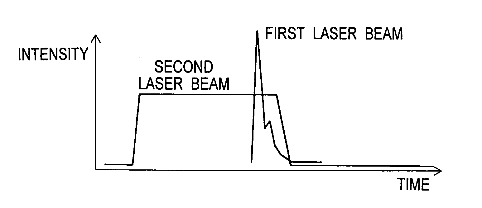
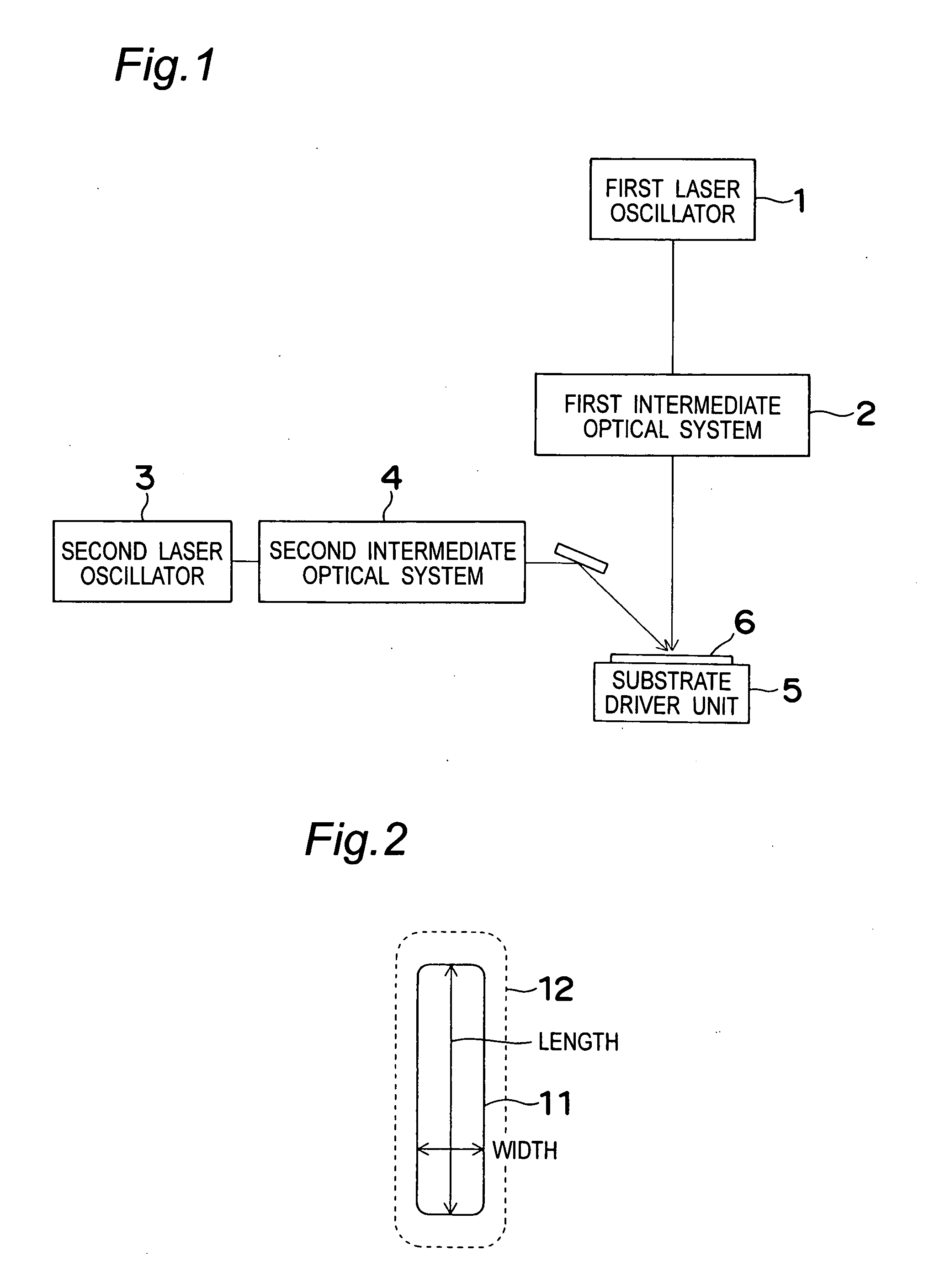
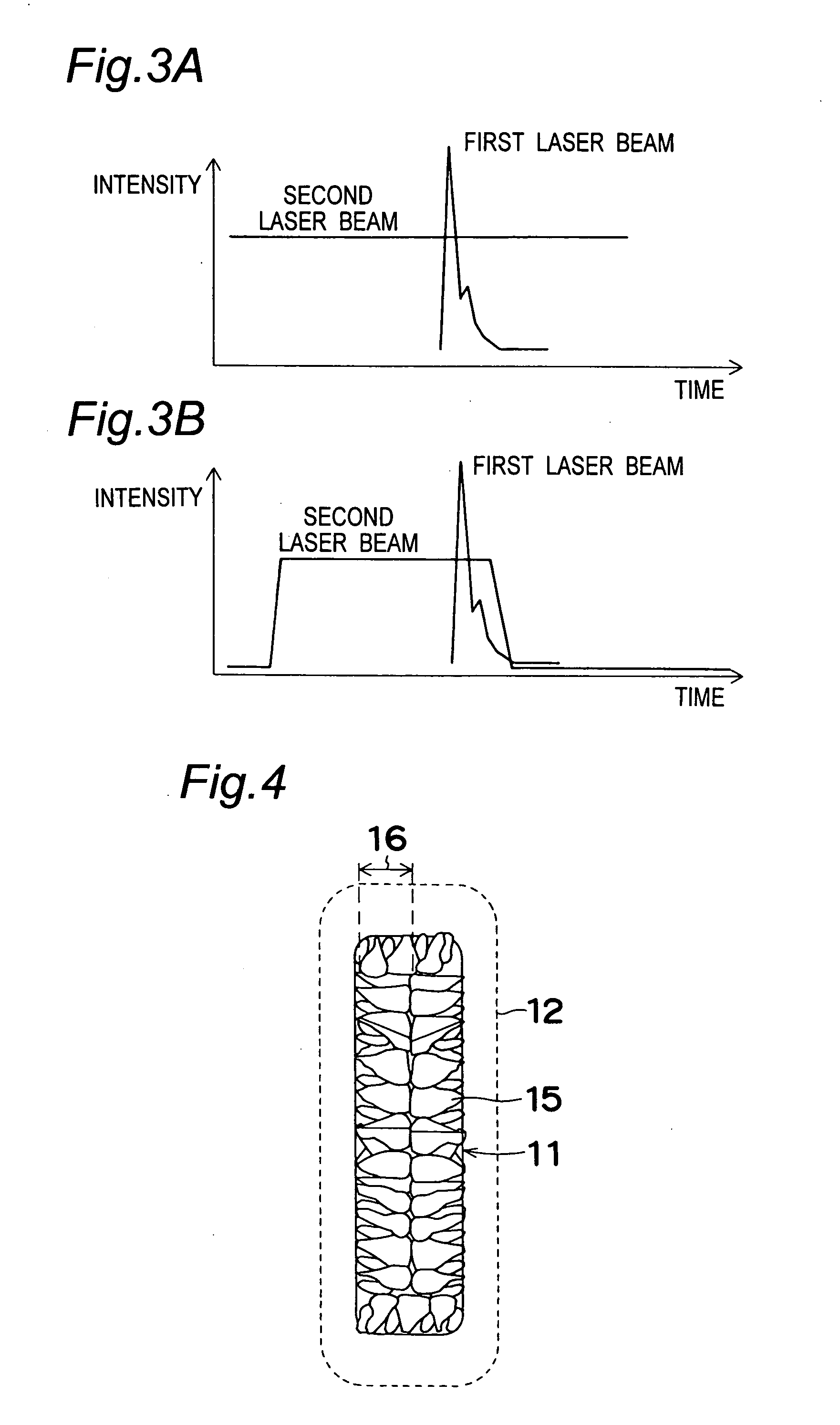
[0069] Hereinbelow, the present invention is described in detail with reference to the accompanying drawings. FIG. 1 is a view showing a configuration of a semiconductor thin film crystallization device of this embodiment. The semiconductor thin film crystallization device is made up a first laser oscillator 1, a first intermediate optical system 2, a second laser oscillator 3, a second intermediate optical system 4 and a substrate drive unit 5. Then, a substrate 6 placed on the substrate driver unit 5 is irradiated with laser beams derived from the first laser oscillator 1 and the second laser oscillator 3.

[0070] The first laser oscillator 1 and the first intermediate optical system 2 constitute an example of the first laser irradiation unit. The second laser oscillator and the second intermediate optical system 4 constitute an example of the second laser irradiation unit. The substrate driver unit 5 constitutes an example of a relative moving unit.

[0071] Although not shown in FI...


PUM

PropertyMeasurementUnit
Angleaaaaaaaaaa
Widthaaaaaaaaaa
Widthaaaaaaaaaa

Abstract

A first laser beam is emitted from a first laser oscillator in a pulsed manner at a high repetition frequency, and converged onto a substrate by a first intermediate optical system 2 so as to form a slit-like first beam spot. A second laser beam is emitted from a second laser beam oscillator in a pulsed manner to rise precedent to and fall subsequent to the first laser beam, and converged onto the substrate by a second intermediate optical system so as to form a second beam spot similar in configuration to the first beam spot and to contain the first beam spot. Crystallization of a semiconductor thin film on the substrate is carried out while the substrate or the first, second beam spots are moved. Thereby, the whole semiconductor thin film is formed into a crystal surface that has grown in one direction and free from ridges. Thus, the semiconductor thin film has an extremely flat surface, extremely few defects, large crystal grains and high throughput.

Description

CROSS-REFERENCE TO RELATED APPLICATIONS [0001] This nonprovisional application claims priority under 35 U.S.C. §119(a) on Patent Application No. 2004-217089 filed in Japan on 26 Jul. 2004, the entire contents of which are incorporated herein by reference. BACKGROUND OF THE INVENTION [0002] The present invention relates to a semiconductor thin film crystallization device and a semiconductor thin film crystallization method, for crystallizing semiconductor thin film by using laser. [0003] In recent years, thin film transistors (hereinafter, referred to as TFTs) using polysilicon film have been drawing attention among TFTs under development. In particular, LCDs (Liquid Crystal Displays) or EL (Electro-Luminescence) Displays employ TFTs in which polysilicon film is used as elements for switching pixels or as elements that form part of the driver circuit for controlling the pixels. [0004] Generally, as the method for obtaining the polysilicon film, amorphous silicon film is crystallized ...

Claims


Application Information

Patent Timeline
IPC IPC(8): H01L21/84H01L21/324H01L21/20
CPCB23K26/0604B23K26/0608B23K26/063B23K26/0732B23K26/0738H01L27/1285H01L21/268H01L29/04H01L29/6675H01L29/78672H01L29/78696H01L21/2026B23K26/0622H01L21/02683H01L21/02686H01L21/02422H01L21/02488H01L21/02678H01L21/02532H01L21/02691H01L21/20H01L21/324H01L21/0268
Inventor INUI, TETSUYANAKAYAMA, JUNICHIROTANIGUCHI, YOSHIHIROSEKI, MASANORITSUNASAWA, HIROSHIKASHIWAGI, IKUMI
Owner SHARP KK
Why Eureka
Try Eureka