Multi-layer wiring structure, semiconductor apparatus having multi-layer wiring structure, and methods of manufacturing them

a multi-layer wiring and semiconductor technology, applied in the direction of semiconductor/solid-state device manufacturing, electric devices, basic electric elements, etc., can solve the problems of poor processability, generation of wiring width variations, and all proposed methods have reliability problems, etc., to achieve high-density buried wiring, low resistance contact can be contrived, and high reliability. , the effect of high-speed operation property

Inactive Publication Date: 2006-01-26
SONY CORP
View PDF4 Cites 97 Cited by
  • Summary
  • Abstract
  • Description
  • Claims
  • Application Information

AI Technical Summary

Benefits of technology

[0036] As has been described above, in the multi-layer wiring structure according to the present invention, even in the case where the second insulation layer is composed of alkyl-containing SiO2 such as SiCOH, the presence of the protective film obviates the inconvenience of erosion of the second insulation layer during the cleaning treatment by hydrogen radicals or hydrogen plasma for cleaning the surface of the first buried wiring fronting on the bottom surface of the wiring connection hole prior to the filling of the wiring connection hole with the connection conductor.
[0037] Therefore, the connection conductor can be formed on the sufficiently cleaned first buried wiring through the wiring connection hole, so that a lower resistance contact can be contrived.
[0038] In addition, since the erosion of the inside surface of the second insulation layer is obviated, the generation of the above-mentioned CD, or variations in the wiring width, can be obviated, so that it is possible to configure a multi-layer wiring structure which has a stable, highly reliable high-density buried wiring desired and which is excellent in high-speed operation property.
[0039] In addition, in the multi-layer wiring structure according to the present invention, at least the second insulation layer has a hybrid structure in which the upper insulation layer provided with the buried wiring has an organic insulation layer lower in dielectric constant than the lower insulation layer provided with the wiring connection hole filled with the connection conductor, and, even in the case of using the organic insulation layer composed of the above-mentioned PAE, for example, the presence of the protective film on the organic insulation layer fronting on the inside of the wiring groove ensures that the erosion of the inside surface is similarly obviated. Therefore, the generation of the above-mentioned CD, or variations in wiring width, can be obviated, and it is possible to configure a multi-layer wiring structure which has a stable, highly reliable high-density buried wiring desired and which is excellent in high speed operation property.
[0040] According to the semiconductor apparatus of the present invention, the multi-layer wiring structure portion thereof has the above-mentioned multi-layer wiring structure according to the present invention, and, therefore, it is possible to configure a semiconductor apparatus which is excellent in high speed operation property and high in reliability.
[0041] According to the method of manufacturing a multi-layer wiring structure and the method of manufacturing a semiconductor apparatus having a multi-layer wiring structure of the present invention, the presence of the protective film ensures that the surface of the first buried wiring to be brought into contact with the connection conductor can be sufficiently cleaned by hydrogen radicals or hydrogen plasma prior to the formation of the connection conductor. Therefore, it is possible to configure a multi-layer wiring structure and a semiconductor apparatus having a multi-layer wiring structure, with excellent characteristics and in high yield.

Problems solved by technology

Since Cu is poor in processability in pattern etching and the like, as in the case of Al, however, Cu wiring based on buried wiring is formed by forming wiring grooves in a layer insulation layer, and applying plating, sputtering or the like to bury Cu into the wiring grooves.
However, a problem as to reliability has been generated in all of the proposed methods.
However, in the cleaning by hydrofluoric acid according to the first method, the removal of the damaged layer generated upon the dry etching leads to the generation of variations in wiring width, i.e., deviations from the designed width, or the so-called CD (Change Dimension).
On the other hand, the cleaning by use of an aqueous solution of organic acid has a problem as to the performance of removal of the etching residue.
When the wiring grooves 108 thus become wider, the adjacent wirings become closer to each other, possibly enhancing the parasitic capacity or causing short circuits, with the result of a lowering in reliability.
In the reduction by hydrogen according to the third method, the reduction of Cu would be insufficient if the resist residue is present.
Besides, in the case of a laminate wiring structure of the dual Damascene structure other than the hybrid structure in which the organic insulation layer of PAE, for example, is used, for example, in the case where alkyl-containing SiO2 such as SiCOH is used as the second insulation layer, the alkyl groups would be drawn out during the cleaning by the hydrogen radicals, leading to deterioration of the electrical and mechanical characteristics of the insulation layer.

Method used


Image

  • Multi-layer wiring structure, semiconductor apparatus having multi-layer wiring structure, and methods of manufacturing them
  • Multi-layer wiring structure, semiconductor apparatus having multi-layer wiring structure, and methods of manufacturing them
  • Multi-layer wiring structure, semiconductor apparatus having multi-layer wiring structure, and methods of manufacturing them

Examples


first embodiment

of the Method of Manufacturing the Multi-layer Wiring Structure

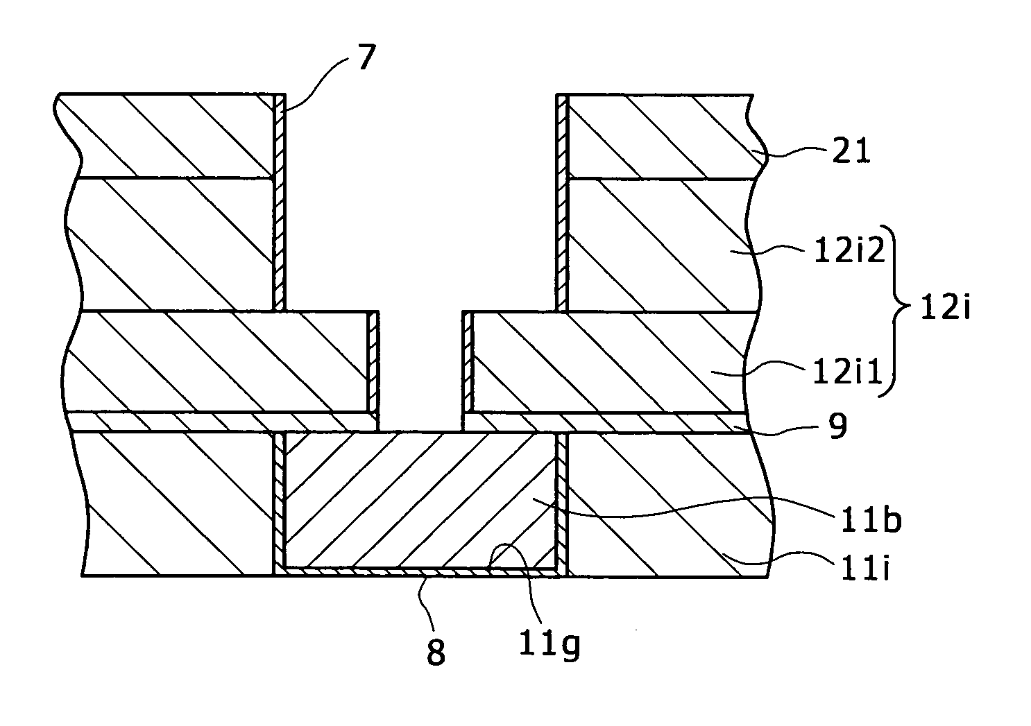
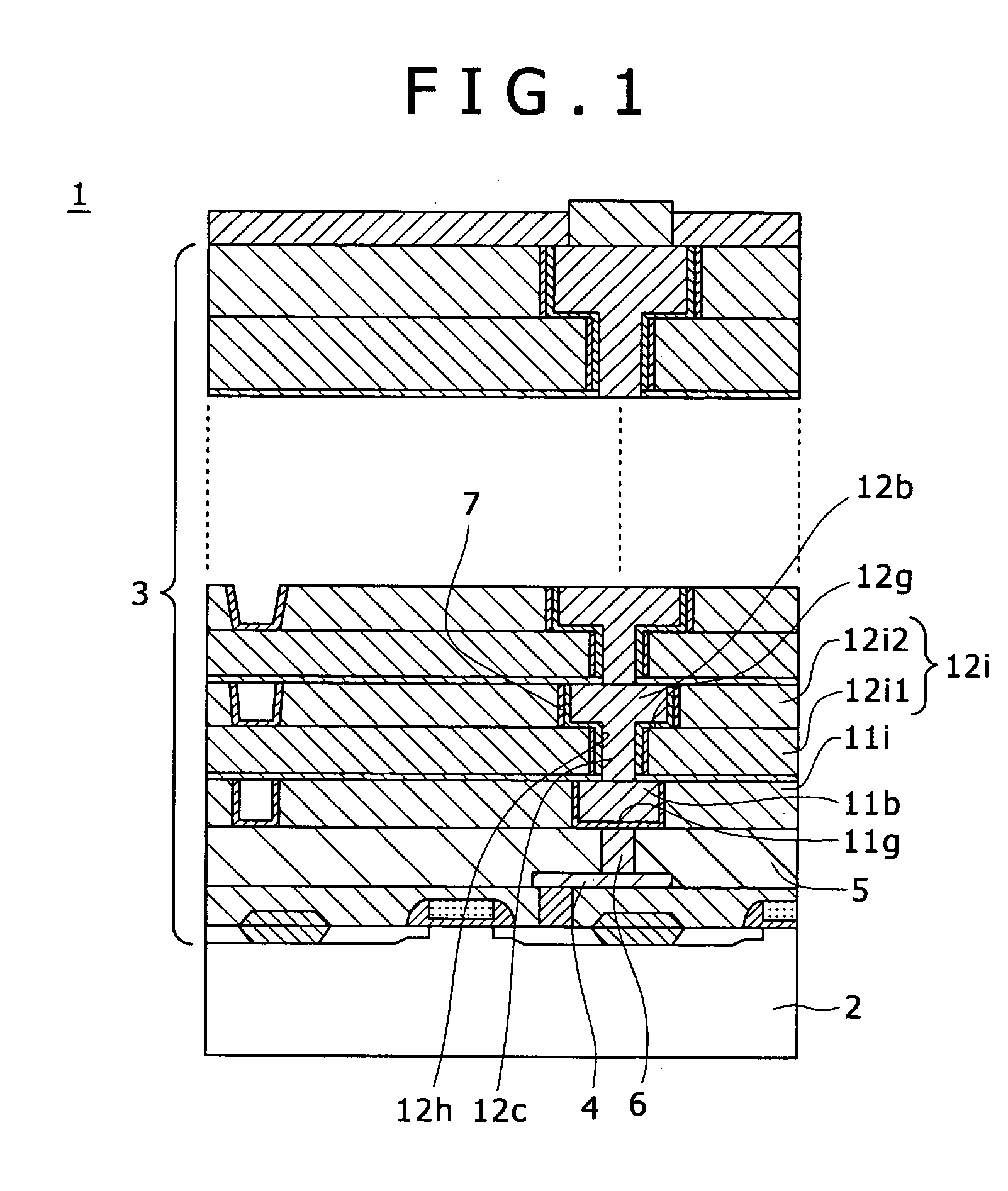
[0071] First, as shown in FIG. 3, the first insulation layer 11i of SiOC, for example, is formed on the flattening insulation layer 5 (not shown) on the semiconductor substrate 2 (not shown) by a PE-CVD (Plasma Enhanced-Chemical Vapor Deposition) process. The above-mentioned first wiring grooves 11g are formed in the first insulation layer 11i by RIE (Reactive Ion Etching) or the like.

[0072] The inside surfaces of the first wiring grooves 11g are coated with a barrier metal layer 8 of SiN, SiC or the like by, for example, sputtering, and the first buried wiring 11b composed of a low-resistance metal, for example, Cu, is formed on the inside surfaces, with the barrier metal layer 8 therebetween. The formation of the buried wiring 11b is conducted by a method in which a layer of Cu, for example, is formed in a thickness sufficiently greater than the depth of the wiring grooves 11g by sputtering, plating or the like, and t...

second embodiment

of the Method of Manufacturing the Multi-Layer Wiring Structure

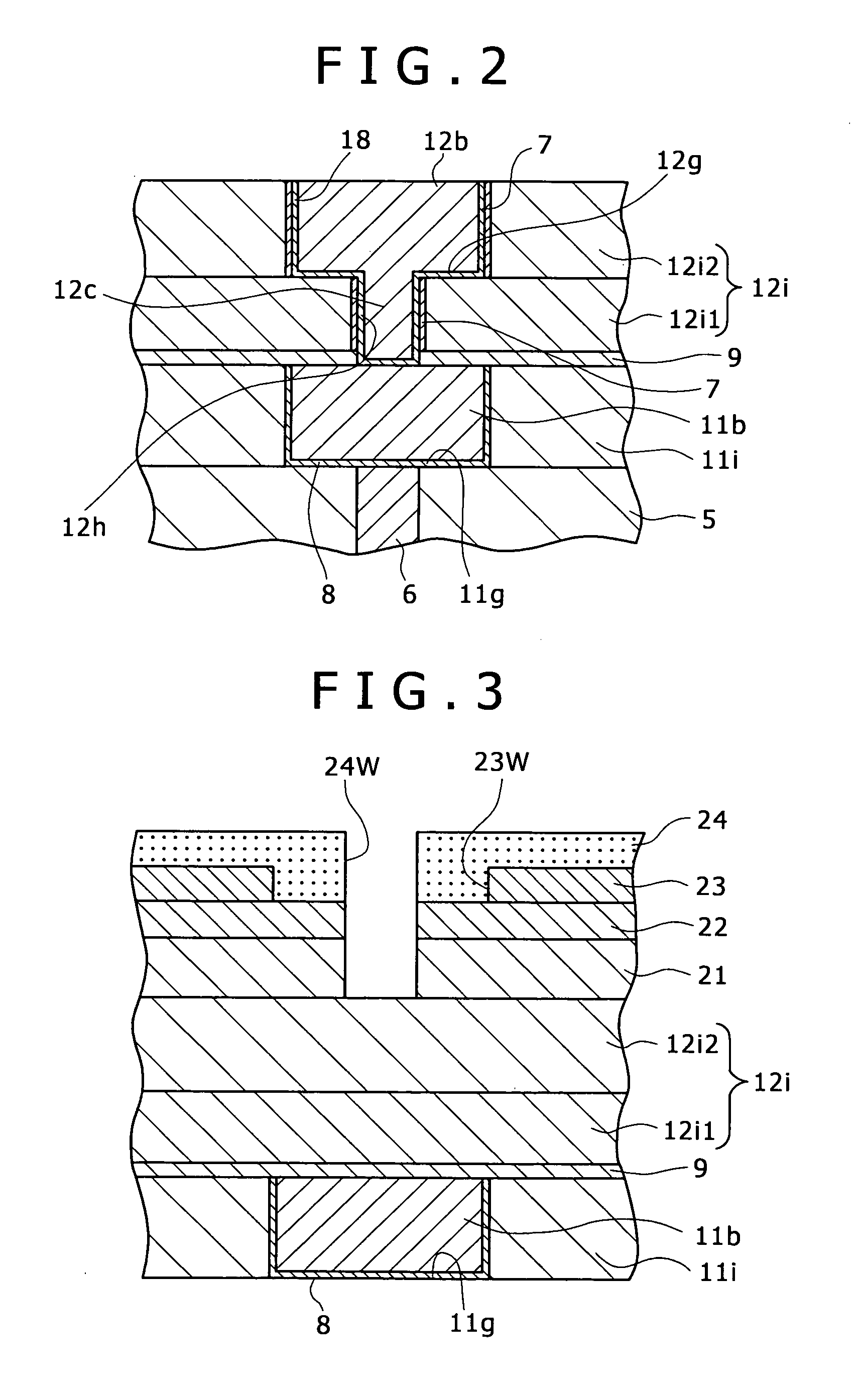
[0099] This embodiment is the case where the protective film 7 is composed of a barrier metal layer 18. In this case, the steps shown in FIGS. 3 to 8 can be performed by adopting the same method as above-described.

[0100] In this case, in place of the formation of the protective film 7 composed of the insulation layer, sputtering of, for example, Ta, TaN, Ti, WN or the like is conducted in a sputtering apparatus for the barrier metal, to form the barrier metal layer 18 as shown in FIG. 12.

[0101] Thereafter, introduction of argon gas and application of a voltage to the substrate 2 in a chamber of the sputtering apparatus are controlled, whereby it is possible to leave the barrier metal layer 18 on the inside surfaces of the second wiring grooves 12g and the wiring connection holes 12h, while enhancing the reverse sputtering for the surfaces intersecting the depth direction thereof so as thereby to remove the barrier meta...


PUM


Abstract

A multi-layer wiring structure including an upper layer wiring (second buried wiring) connected to a buried wiring (first buried wiring) in lower layer wiring grooves (first wiring grooves) through connection conductors, wherein a protective film capable of enduring a cleaning treatment with hydrogen radicals or hydrogen plasma applied to the surface of the first buried wiring at the time of forming the connection conductors is formed on the inside surfaces of the wiring grooves to be filled with he second buried wiring and the wiring connection holes to be filled with the connection conductors which surfaces are liable to be eroded upon exposure to the atmosphere used in the cleaning treatment, whereby erosion of the insulation layers at the time of the cleaning is obviated, sufficient cleaning can be performed, and deterioration of characteristics can be improved.

Description

BACKGROUND OF THE INVENTION [0001] The present invention relates to a multi-layer wiring structure, a semiconductor apparatus having a multi-layer wiring structure, and methods of manufacturing them. [0002] For example, in semiconductor integrated circuit apparatuses, there is a need for more and more higher speed, smaller power consumption, smaller size and higher degree of integration, and, according to this, there is a need for more and more higher accuracy, higher degree of multiplicity of layers, lower wiring resistance, and larger reduction in mutual parasitic capacity of wirings. [0003] To contrive a lower wiring resistance, Cu wiring with low resistance is adopted in place of Al used in ordinary wirings. Since Cu is poor in processability in pattern etching and the like, as in the case of Al, however, Cu wiring based on buried wiring is formed by forming wiring grooves in a layer insulation layer, and applying plating, sputtering or the like to bury Cu into the wiring groove...

Claims


Application Information

Patent Timeline
Patent Type & Authority Applications(United States)
IPC IPC(8): H01L21/4763
CPCH01L21/76811H01L21/76813H01L21/76814H01L21/76862H01L21/76835H01L21/76844H01L21/76831
Inventor KOMAI, NAOKIHAYASHI, TOSHIHIKO
Owner SONY CORP
Why Eureka
Try Eureka