

Plasma processing method and application thereof
A plasma and processing method technology, applied in the field of plasma processing, can solve problems such as direction deviation, lattice defects, and high barrier height, etc., and achieve the effect of reducing the surface state density and improving the quality of the surface or interface
- Summary
- Abstract
- Description
- Claims
- Application Information
AI Technical Summary
Problems solved by technology
Method used
Image

Examples
Embodiment 1
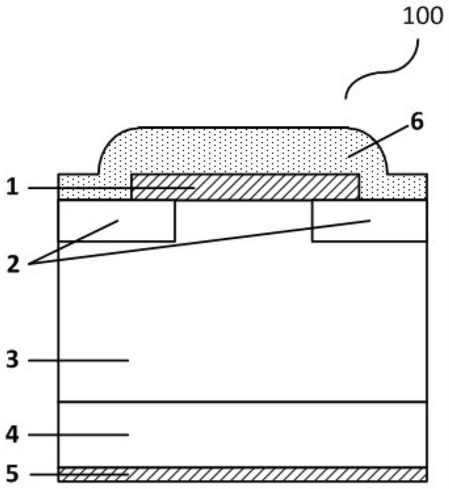
[0045] figure 1 It is a schematic cross-sectional structure diagram 100 of a GaN Schottky diode according to Embodiment 1 of the present invention, as figure 1 In the implementation shown, the Schottky diode includes an anode metal 1 , a barrier modulation region 2 , an N-type drift region 3 , an N-type substrate 4 , a cathode 5 , and a dielectric layer 6 . The GaN Schottky diode 100 is subjected to surface barrier modulation only at the peripheral portion where the barrier modulation region 2 contacts the anode metal 1 , for example, the peripheral portion where the anode 1 contacts the N-type drift region 3 . Such as figure 1 In the shown embodiment, the barrier height at the edge of the anode metal 1 is increased, so as to reduce the reverse leakage current of the device and improve the reverse withstand voltage of the device.
[0046] The barrier modulation method specifically refers to treating the surface of the power device with, but not limited to, plasma gas contain...
Embodiment 2
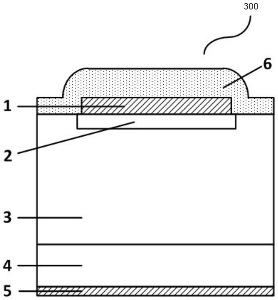
[0058] Such as Figure 4 In the shown embodiment 2, the barrier height of the entire contact surface between the anode metal 1 and the N-type drift region 3 is increased, thereby increasing the turn-on voltage of the device and enhancing the switching performance of the device.
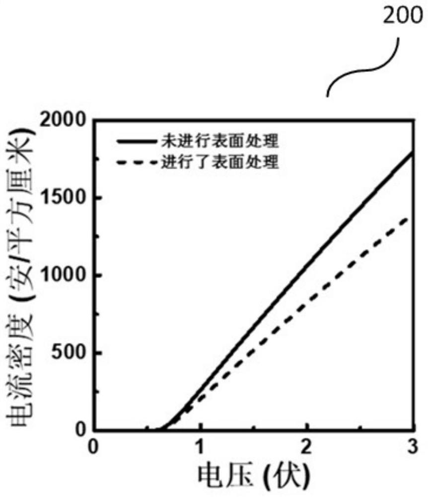
[0059] Figure 5 for Figure 4 The structure shown is a comparison diagram of forward conduction characteristics of the device before and after performing the surface barrier modulation processing method obtained through simulation. Wherein, the thickness of the N-type drift region 3 is 11 μm, and its doping concentration is ~8×10 15 cm -3 ; N-type substrate 4 doping concentration is ~ 1 × 10 18 cm -3 .
[0060] It can be found that after the surface barrier modulation treatment is performed on the contact surface between the entire barrier modulation region 2 and the anode metal 1 of the semiconductor power device, the forward turn-on voltage of the device will be significantly improved, so for...
Embodiment 3
[0070] Figure 6 It is a cross-sectional view of a GaN PiN diode 600 according to Embodiment 3 of the present invention. Such as Figure 6 In the illustrated embodiment, the GaN PiN diode 600 includes a P-type GaN layer surface treatment region 7, an anode 8, a P-type GaN layer 9, an N-type GaN layer 10, a substrate 11, and a cathode 12 and dielectric layer 13. The substrate 11 includes, but is not limited to, gallium nitride, silicon carbide, silicon, sapphire, silicon-on-insulator (SOI), aluminum nitride, aluminum gallium nitride (Al x Ga 1-x One or more of N, 0<x<1), diamond, metal copper, metal silver and metal aluminum; the N-type gallium nitride layer 10 is located above the substrate 11; the P-type gallium nitride layer Layer 9 is located above the N-type GaN layer 10; the P-type GaN layer surface treatment region 7 is located on the surface of the P-type GaN layer 9; the anode 8 is located on the P-type GaN layer Above the layer surface treatment region 7, the ano...
PUM
| Property | Measurement | Unit |
|---|---|---|
| thickness | aaaaa | aaaaa |
| thickness | aaaaa | aaaaa |
Abstract
Description
Claims
Application Information