Method of forming low resistance and reliable via in inter-level dielectric interconnect

a dielectric interconnect and low resistance technology, applied in the manufacturing of semiconductor/solid-state devices, basic electric elements, electric apparatus, etc., can solve the problems of interconnect delay, contaminating the lower conductive layer, interconnect delay becomes one of the most significant limiting factors of integrated circuit performance, etc., to improve resistivity, improve resistivity, and reduce resistance

Inactive Publication Date: 2007-05-29
GLOBALFOUNDRIES INC
View PDF6 Cites 0 Cited by
  • Summary
  • Abstract
  • Description
  • Claims
  • Application Information

AI Technical Summary

Benefits of technology

[0009]This invention addresses directly a method for cleaning and passivating a conductor surface at the bottom of an interconnection via, so as to form a low resistance contact at the bottom of a via and improve the reliability of the via.
[0012]A second aspect of the invention is directed to a contact structure for connecting a conducting layer formed in a semiconductor device to a subsequent conducting layer through an interlevel dielectric material. The contact structure comprises a via structure formed over the conducting layer, the conducting layer comprising a copper metal having a surface region including a concentration of implanted Nitrogen ions; and, a thin refractory metal liner material formed over the region having the concentration of implanted Nitrogen ions at a bottom of the via structure and along sidewall of the structure; and, a metal plug formed in said via structure, wherein the contact via structure exhibits improved resistivity. Preferably, the inert gas includes Nitrogen which reacts with an underlying exposed Copper metal to form a thin layer of CuN. The contact via structure exhibits improved resistivity.
[0013]Besides forming a contact structure of lower resistance, the passivation of the metal surface and formation of CuN at the location of an interlevel contact via according to the invention advantageously results in increased adhesion with the subsequently formed metal contact liner, thus improving reliability of the contact.

Problems solved by technology

With semiconductor technology scaling down below sub-quarter micron, interconnect delay (RC delay) becomes one of the most significant limiting factor for performance of an integrated circuit.
The sputter clean process of the prior art, however, may itself cause problems with the interconnect, in particular when a carbon containing low-k ILD is used.
One disadvantage of the prior art is that carbon containing low-k ILD material may be dislodged from the sidewalls of the hole when plasma ions collide with the sidewalls, and then may deposit on and contaminate the lower conductive layer and increase contact resistance.
Another disadvantage of the prior art is that the re-deposited carbon containing byproduct may degrade the adhesion of the liner or plug to the underlying conductive layer.
In addition, the re-deposited carbon containing material may cause interconnect reliability problems, such as interconnect resistance shift during thermal stress.
However, even after cleaning of the via, the metal surface may further be exposed to the ambient (atmosphere or in vacuum) when the wafer is moved between the pre-clean chamber and deposition chamber for the metallization of the vias.
In these instances, the metal layer adsorb contaminants from the ambient, these contaminates (i.e. oxygen, carbon) react with the top of the metal layer and create a resistive layer that hinders the electrical connectivity of the metal layer and affects the electrical contact and reliability of the vias.

Method used


Image

  • Method of forming low resistance and reliable via in inter-level dielectric interconnect
  • Method of forming low resistance and reliable via in inter-level dielectric interconnect
  • Method of forming low resistance and reliable via in inter-level dielectric interconnect

Examples


Embodiment Construction

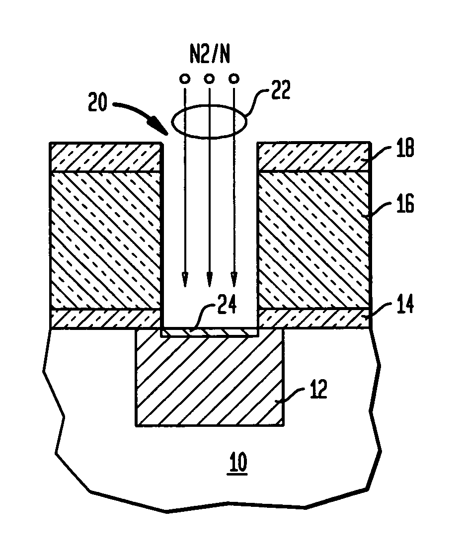
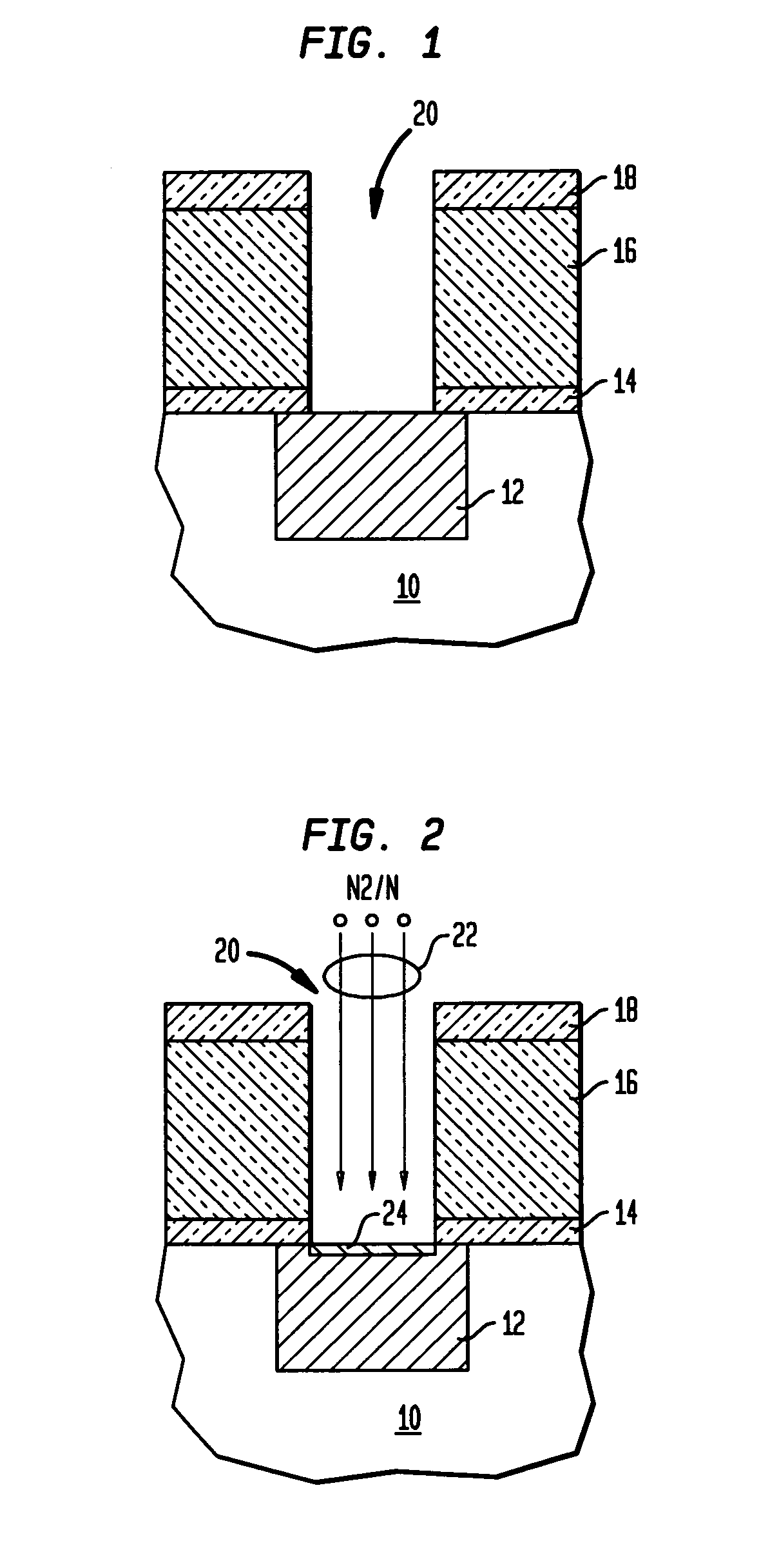
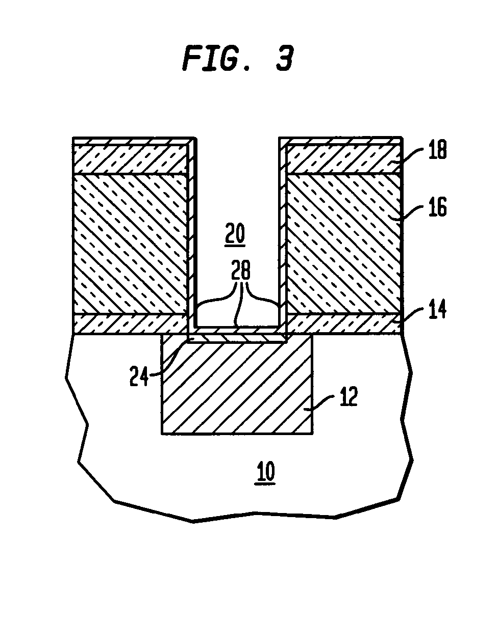
[0019]With reference to the accompanying drawings, FIGS. 1–3 illustrate schematic cross-sectional representations of methods of cleaning and passivating the Cu surface and depositing a refractory liner with a low contact resistance in at least one via of a semiconductor device according to the invention.

[0020]As shown in FIG. 1, there is provided a substrate 10 which may be a bulk semiconductor including, for example, Si, SiGe, SiC, SiGeC, GaAs, InP, InAs and other semiconductors, or layered semiconductors such as silicon-on-insulators (SOI), SiC-on-insulator (SiCOI) or silicon germanium-on-insulators (SGOI). When the layered semiconductors are employed, the top layer of those substrates represent the top layer 10 shown in FIG. 1. Formed on substrate 10 is a representative metal layer (M1) layer 12 which may be a patterned wiring level of conducting material such as Cu, Al, or alloys thereof. Atop of the metal layer is a subsequently formed bottom dielectric capping layer 14 which m...


PUM

PropertyMeasurementUnit
thicknessaaaaaaaaaa
dielectric constantaaaaaaaaaa
porosityaaaaaaaaaa

Abstract

A novel interlevel contact via structure having low contact resistance and improved reliability, and method of forming the contact via. The method comprises steps of: etching an opening through an interlevel dielectric layer to expose an underlying metal (Copper) layer surface; and, performing a low energy ion implant of an inert gas (Nitrogen) into the exposed metal underneath; and, depositing a refractory liner into the walls and bottom via structure which will have a lower contact resistance due to the presence of the proceeding inert gas implantation. Preferably, the inert Nitrogen gas reacts with the underlying exposed Copper metal to form a thin layer of CuN.

Description

FIELD OF THE INVENTION[0001]The present invention related generally to the fabrication of semiconductor circuit devices, and more particularly to a novel method for improving the resistance and reliability of redundancy via in a copper (Cu) interconnect.BACKGROUND OF THE INVENTION[0002]Semiconductor devices typically include interconnects, such as vias and contacts, which connect conductive elements in non-successive layers within a semiconductor device. A via generally connects two metallic elements in different layers of a semiconductor device. A contact generally connects metallic and non-metallic conducting or semiconducting (such as silicon, polysilicon, or silicide) elements in different layers of a semiconductor device. As used herein, a “conductive” element or layer is defined to include both conducting and semiconducting elements or layers. The interconnect is typically formed in an inter-level dielectric (“ILD”) layer disposed between the layers to be connected. With semic...

Claims


Application Information

Patent Timeline
Patent Type & Authority Patents(United States)
IPC IPC(8): H01L21/44
CPCH01L21/76843H01L21/76849H01L21/76867H01L21/76888
Inventor CABRAL, JR., CYRILCLEVENGER, LAWRENCE A.DALTON, TIMOTHY J.DEHAVEN, PATRICK W.DZIOBKOWSKI, CHESTER T.FANG, SUNFEISPOONER, TERRY A.TAI, TSONG-LIN L.WONG, KWONG HONYANG, CHIN-CHAO
Owner GLOBALFOUNDRIES INC
Why Eureka
Try Eureka