Post passivation interconnection schemes on top of the IC chips

a technology of interconnection schemes and ic chips, applied in the direction of semiconductor devices, semiconductor/solid-state device details, electrical devices, etc., can solve the problem that two approaches cannot create thick metal, and achieve the effect of high resistivity of interconnection lines

Inactive Publication Date: 2006-02-23
QUALCOMM INC
View PDF44 Cites 33 Cited by
  • Summary
  • Abstract
  • Description
  • Claims
  • Application Information

AI Technical Summary

Benefits of technology

[0029] A principal objective of the invention is to provide a method for the creation of interconnect metal that allows for the use of thick and wide metal.
[0031] Yet another objective of the invention is to provide a method that allows for the creation of long interconnect lines, whereby these long interconnect lines do not have high resistance or introduce high parasitic capacitance.

Problems solved by technology

This because an inorganic material cannot be deposited as a thick layer of dielectric because such a layer of dielectric would develop fissures and crack as a result fine-line interconnect metal is typically created using methods of sputter with resist etching or of damascene processes using oxide etch with electroplating after which CMP is applied.
Either one of these two approaches cannot create thick metal due to cost considerations or oxide cracking thick, wide interconnect lines can be created by first sputtering a thin metal base layer, coating and patterning a thick layer of photoresist, applying a thick layer of metal by electroplating, removing the patterned photoresist and performing metal base etching (of the sputtered thin metal base).

Method used


Image

  • Post passivation interconnection schemes on top of the IC chips
  • Post passivation interconnection schemes on top of the IC chips
  • Post passivation interconnection schemes on top of the IC chips

Examples


Embodiment Construction

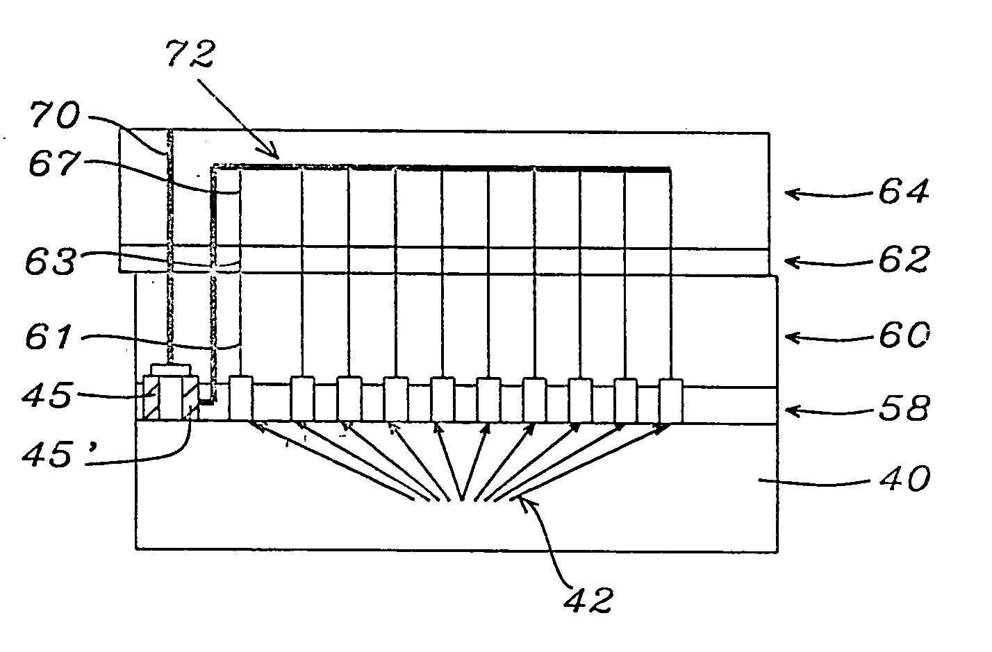
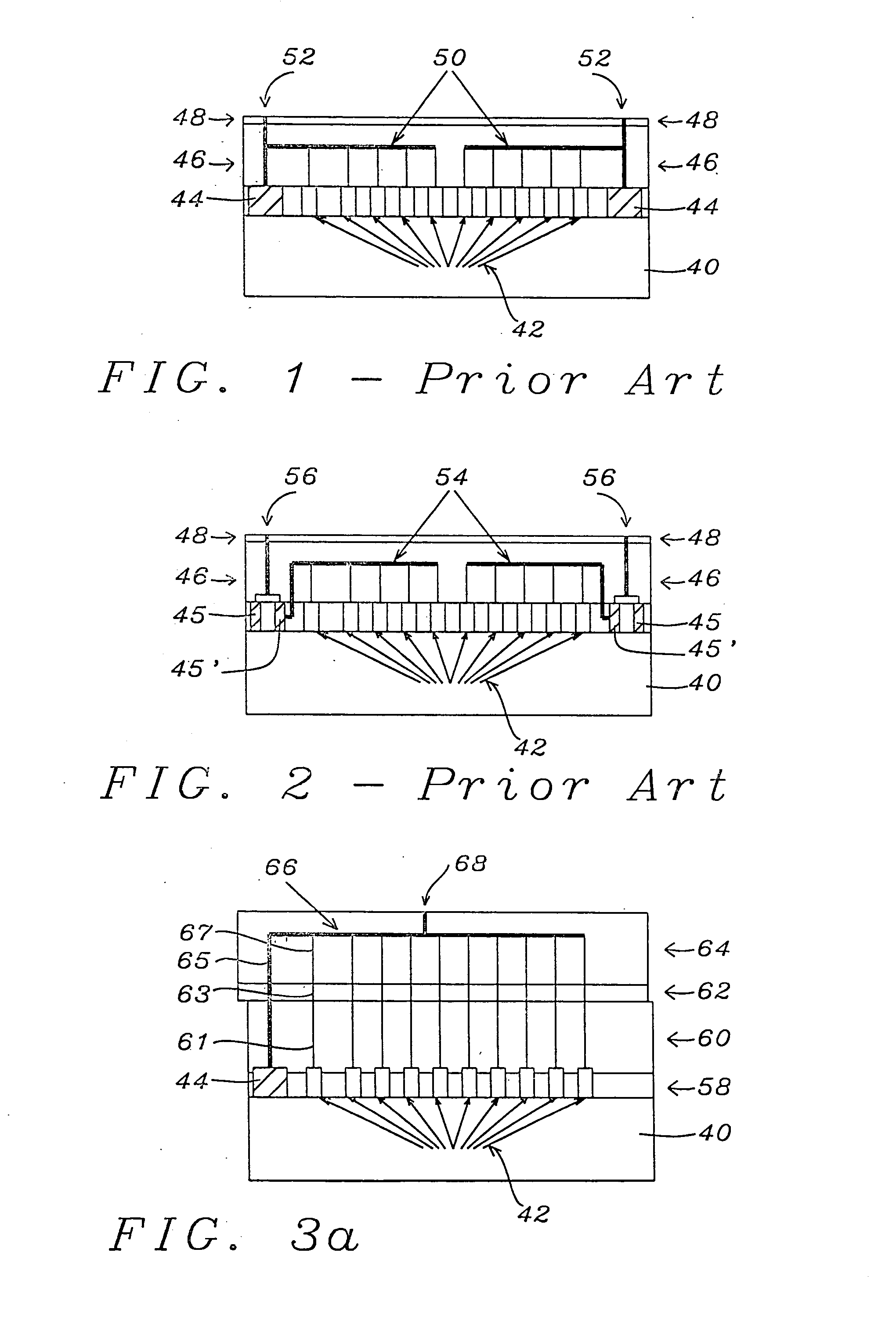
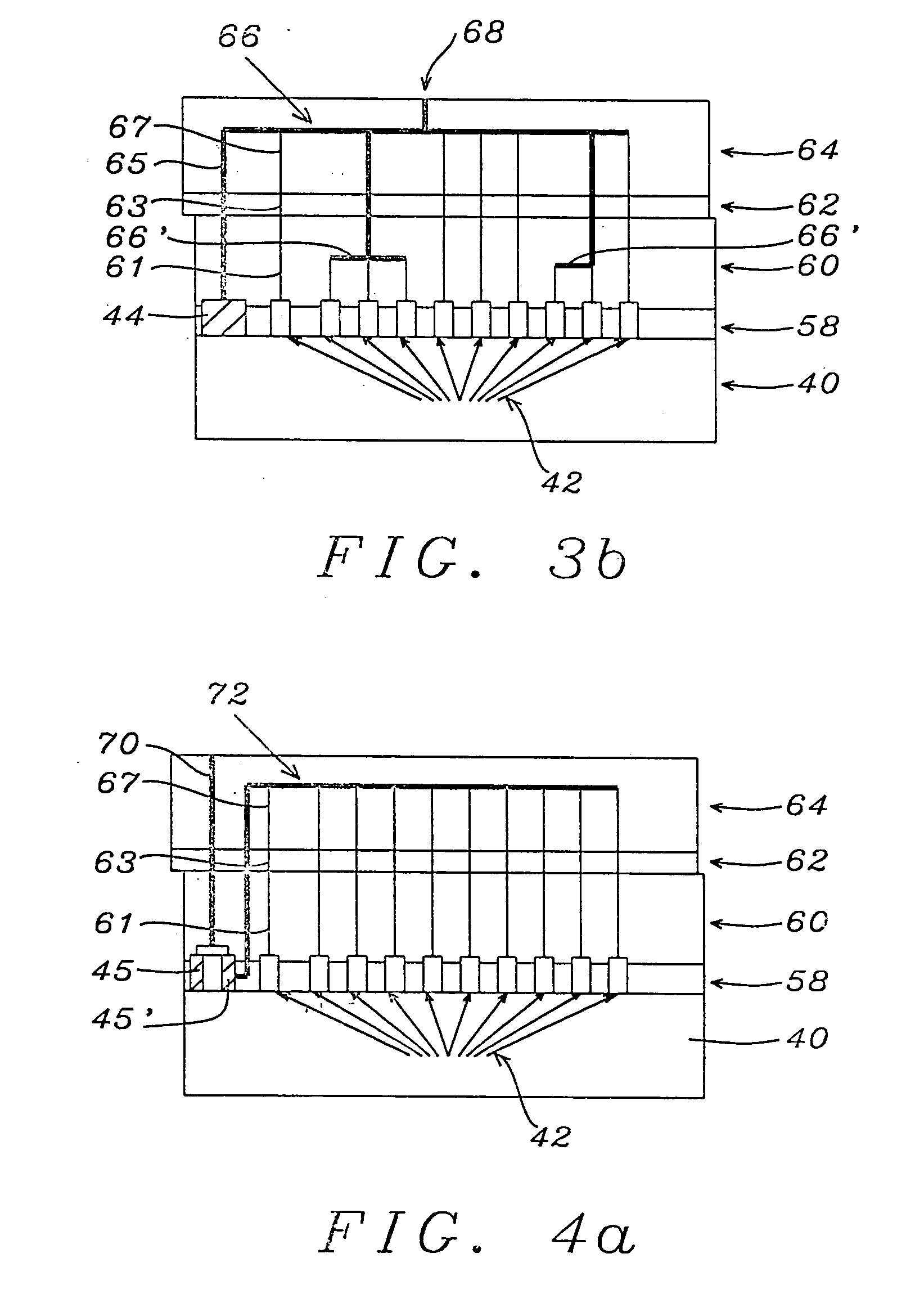
[0046] For purposes of reference and for clarity of understanding, FIG. 6, is taken from related application Ser. No. 09 / 251,183 and is herein incorporated by reference.

[0047] Referring now more specifically to FIG. 6, there is shown a cross section of one implementation of the referenced application. The surface of silicon substrate 10 has been provided with transistors and other devices (not shown in FIG. 6). The surface of substrate 10 is covered by a dielectric layer 12, layer 12 of dielectric is therefore deposited over the devices that have been provided in the surface of the substrate and over the substrate 10. Conductive interconnect lines 11 are provided inside layer 12 that connect to the semiconductor devices that have been provided in the surface of substrate 10.

[0048] Layers 14 (two examples are shown) represent all of the metal layers and dielectric layers that are typically created on top of the dielectric layer 12, layers 14 that are shown in FIG. 6 may therefore c...


PUM


Abstract

A new method is provided for the creation of interconnect lines. Fine line interconnects are provided in a first layer of dielectric overlying semiconductor circuits that have been created in or on the surface of a substrate. A layer of passivation is deposited over the layer of dielectric, a thick second layer of dielectric is created over the surface of the layer of passivation. Thick and wide interconnect lines are created in the thick second layer of dielectric. The first layer of dielectric may also be eliminated, creating the wide thick interconnect network on the surface of the layer of passivation that has been deposited over the surface of a substrate.

Description

RELATED PATENT APPLICATIONS [0001] This application is related to Ser. No. 09 / 251,183 filed on Feb. 17, 1999 which is a continuation-in-part of Ser. No. 09 / 216,791 filed on Dec. 21, 1998 assigned to a common assignee. This application is also related to attorney docket MEG00-008, Ser. No. ______, filing date ______.BACKGROUND OF THE INVENTION [0002] (1) Field of the Invention [0003] The invention relates to the fabrication of integrated circuit devices, and more particularly, to a method of post-passivation processing for the creation of conductive interconnects. [0004] (2) Description of the Prior Art [0005] Improvements in semiconductor device performance are typically obtained by scaling down the geometric dimensions of the Integrated Circuits, this results in a decrease in the cost per die while at the same time some aspects of semiconductor device performance are improved. The metal connections which connect the Integrated Circuit to other circuit or system components become of...

Claims


Application Information

Patent Timeline
Patent Type & Authority Applications(United States)
IPC IPC(8): H01L23/62H01L21/768H01L23/528H01L23/532H01L23/60H01L27/02
CPCH01L21/768H01L24/05H01L21/76838H01L23/5222H01L23/5223H01L23/5227H01L23/5283H01L23/5286H01L23/5329H01L23/53295H01L23/60H01L23/62H01L27/0248H01L2924/12044H01L2924/3011H01L21/76801H01L2924/12042H01L2924/14H01L2924/0002H01L2924/00
Inventor LIN, MOU-SHIUNGLEE, JIN-YUAN
Owner QUALCOMM INC
Why Eureka
Try Eureka