Method for manufacturing display device

Inactive Publication Date: 2006-03-02
SEMICON ENERGY LAB CO LTD
View PDF1 Cites 79 Cited by
  • Summary
  • Abstract
  • Description
  • Claims
  • Application Information

AI Technical Summary

Benefits of technology

[0017] According to the present invention, a top-gate type thin film transistor with a planar structure that has a crystalline semiconductor film can be formed. A TFT having a crystalline semiconductor film formed according to the present invention has higher mobility compared to a TFT formed using an amorphous semiconductor film. Also, the source region and the drain region include a metal element that promotes the crystallization, in addition to an impurity element imparting a p-type conductivity (an acceptor element) or an impurity element imparting an n-type conductivity (a donor element). Accordingly, a source region and a drain region having low resistivity can be formed. As a consequence, a display device that is necessary to be operated at high speed can be manufactured.
[0018] As compared to a thin film transistor

Problems solved by technology

In particular, development of large-area liquid crystal television devices equipped with large-size active matrix liquid crystal panels has been a major issue for liquid crystal panel manufacturers.
Meanwhile, the conventional liquid crystal television devices have defects of image deblurring caused by the limits of viewing angle characteristics and the limits of high-speed operation due to a liquid crystal

Method used


Image

  • Method for manufacturing display device
  • Method for manufacturing display device
  • Method for manufacturing display device

Examples


embodiment mode 1

[0069] The embodiment modes according to the present invention will hereinafter be described referring to the accompanying drawings. It is easily understood by those who skilled in the art that the embodiment modes and details herein disclosed can be modified in various ways without departing from the purpose and the scope of the invention. The present invention should not be interpreted as being limited to the description of the embodiment modes to be given below. Identical portions or portions having similar functions are marked by same reference numerals throughout the drawings so as to eliminate repeated explanation.

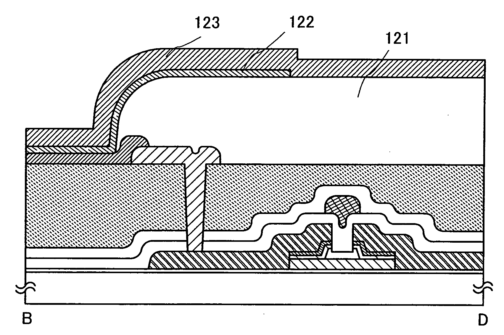
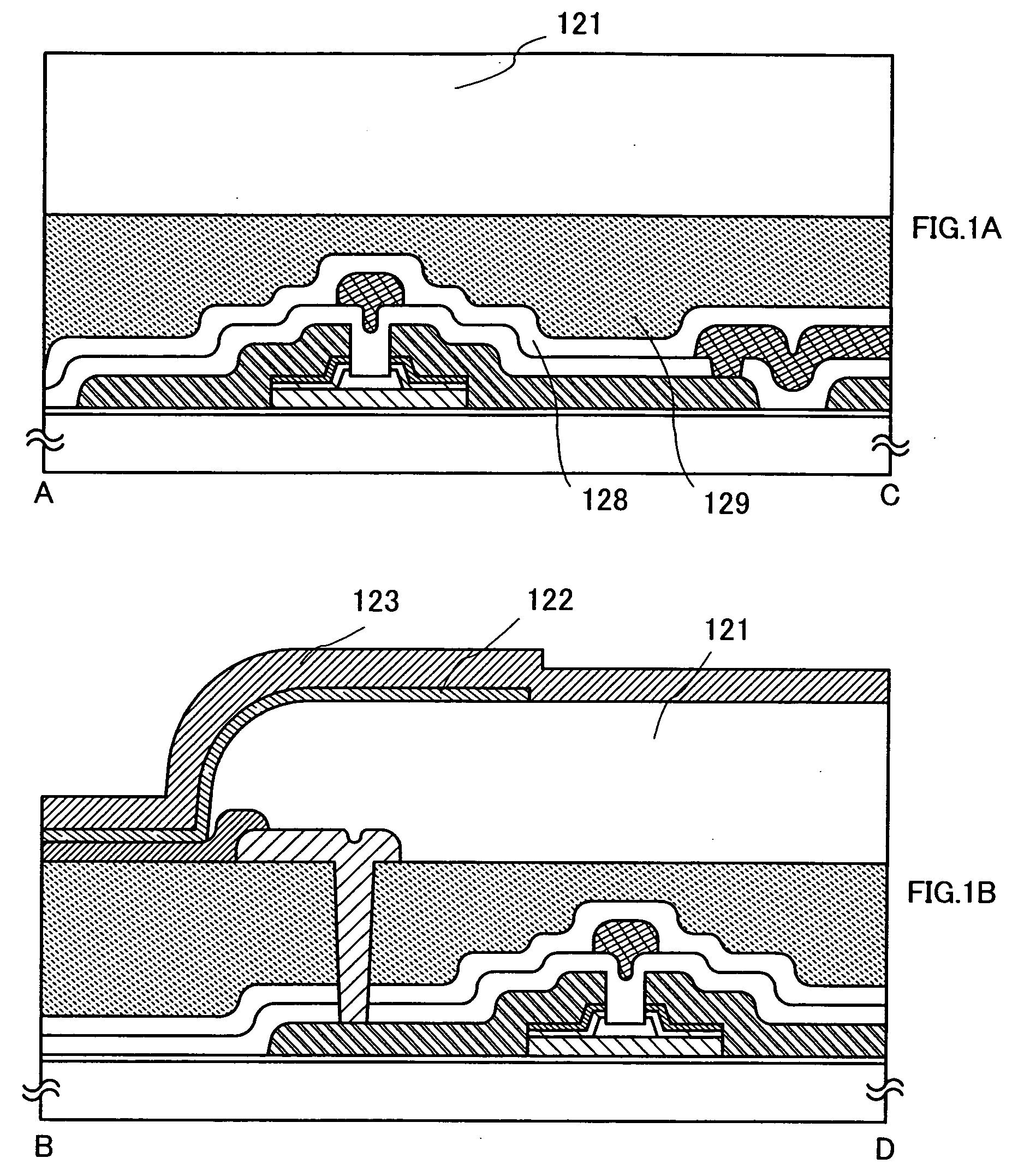
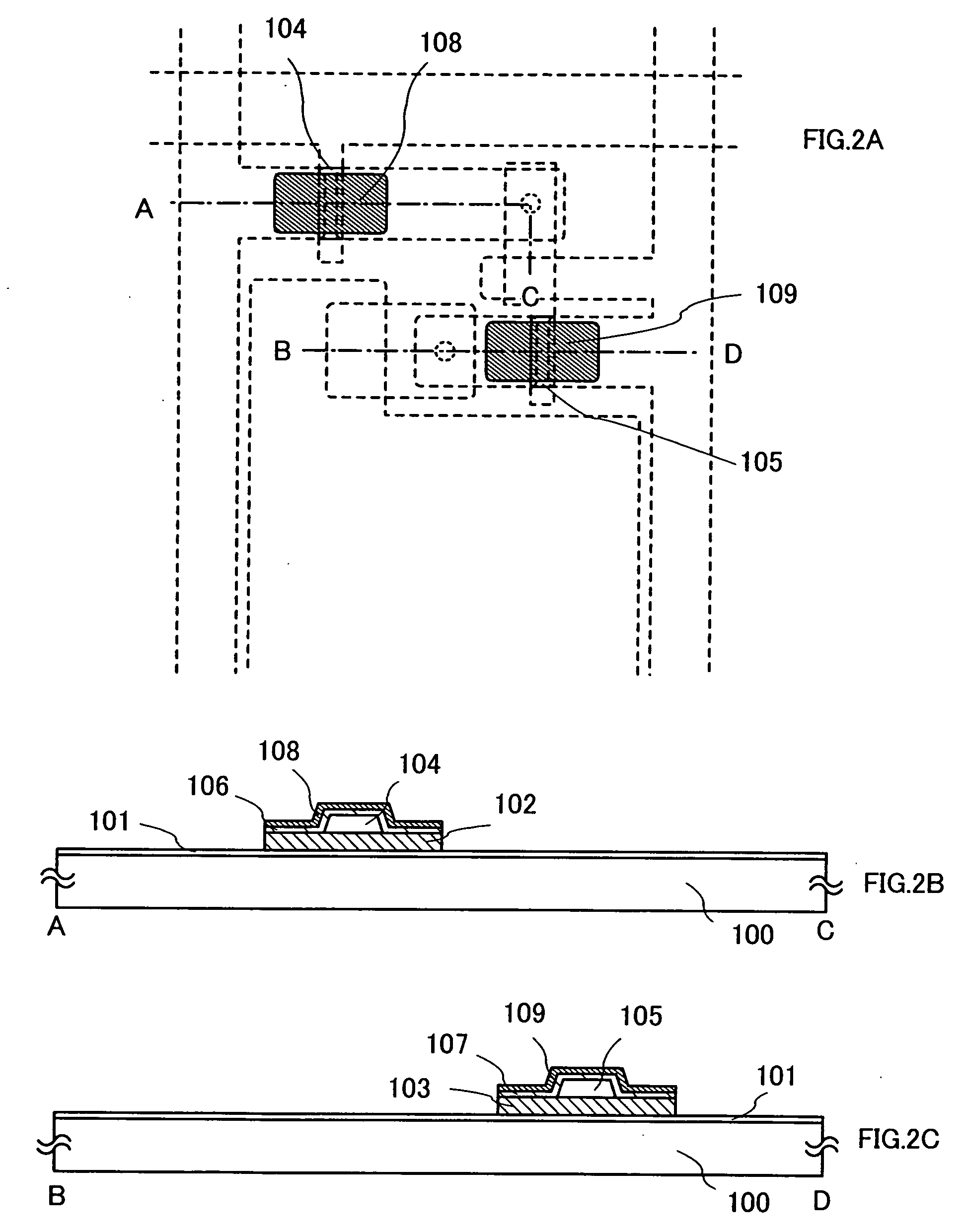
[0070]FIG. 33A is a top view showing a structure of a display panel according to the present invention. A pixel portion 2701 over which pixels 2702 are arranged in matrix form, a scanning line input terminal 2703 and a signal line input terminal 2704 are formed over a substrate 2700 with an insulated surface. The number of pixels may be determined in accordance with...

embodiment mode 2

[0162] Another embodiment mode of the present invention will be described with reference to FIGS. 8A to 8F. This embodiment mode shows an example of manufacturing a circuit that includes a plurality of n-channel thin film transistors (NMOS) through a gettering step that is different from the gettering step carried out in manufacturing the thin film transistor of Embodiment Mode 1. Therefore, identical portions and portion having identical functions to those of Embodiment Mode 1 will not be further explained in this embodiment mode.

[0163] An insulating layer 401 and an amorphous semiconductor film 402 are formed over a substrate 400. A metal film 403 containing a metal element that promotes crystallization (which is nickel (Ni) in this embodiment mode) is formed thereon (see FIG. 8A). Thereafter, the amorphous semiconductor film 402 is crystallized by a heat treatment to form a crystalline semiconductor film 404.

[0164] In this embodiment mode, after selectively forming a channel pr...

embodiment mode 3

[0170] Another embodiment mode of the invention will be described with reference to FIGS. 9A to 9E. The present embodiment mode shows an example of manufacturing a circuit including a plurality of p-channel thin film transistors (PMOS) that are formed through different gettering step from the gettering step carried out in forming the thin film transistor of Embodiment Mode 1. The identical portions and portions having identical functions to those of Embodiment Mode 1 will not be further explained in this embodiment mode.

[0171] An insulating layer 401 and an amorphous semiconductor film 402 are formed over a substrate 400. A metal film 403 containing a metal element for promoting crystallization (which is nickel (Ni) in this embodiment mode) is formed thereon (see FIG. 9A). Thereafter, the amorphous semiconductor film 402 is crystallized by a heat treatment to form a crystalline semiconductor film 404.

[0172] A semiconductor film 405 containing a rare gas element as an impurity elem...


PUM


Abstract

The present invention provides a method for manufacturing a display device having a TFT that can be operated at high speed while using a small number of photomasks and improving the utilization efficiency of materials, where the threshold value is difficult to be varied. In the invention, a catalytic element is applied to an amorphous semiconductor film and the amorphous semiconductor film is heated to form a crystalline semiconductor film. After removing the catalytic element from the crystalline semiconductor film, a top-gate type thin film transistor with a planar structure is manufactured. Moreover, by using the droplet discharging method where an element of a display device is formed selectively, the process can be simplified, and loss of materials can be reduced.

Description

BACKGROUND OF THE INVENTION [0001] 1. Field of the Invention [0002] The present invention relates to a method for manufacturing a display device. [0003] 2. Description of the Related Art [0004] In recent years, flat panel displays (FPDs) typified by liquid crystal displays (LCDs) and electroluminescent (EL) displays have been attracting attention as display devices taking the place of the conventional CRTs. In particular, development of large-area liquid crystal television devices equipped with large-size active matrix liquid crystal panels has been a major issue for liquid crystal panel manufacturers. Moreover, development of large-area EL television devices has recently been carried out following to the development of the liquid crystal television devices. [0005] A thin film transistor (hereinafter, also referred to as a TFT) using an amorphous silicon is used as a semiconductor element for driving each pixel in the conventional liquid crystal display device or EL display device (...

Claims


Application Information

Patent Timeline
IPC IPC(8): H01L21/00
CPCH01L27/322H01L27/1292H01L27/3246H01L27/3262H01L27/3276H01L29/42384H01L29/458H01L29/66757H01L29/78675H01L29/78696H01L51/0005H01L51/5237H01L51/5281H01L51/529H01L51/56H01L2251/5315H01L2251/5323H01L27/1277H01L27/3244Y02P80/30H10K59/38H10K59/1213H10K71/135H10K59/122H10K59/12H10K59/131H10K50/841H10K50/87H10K50/86H10K2102/3031H10K2102/3026H10K50/844H10K71/00
Inventor SHOJI, HIRONOBUMAEKAWA, SHINJIYOSHIZUMI, KENSUKEHONDA, TATSUYASUZUKI, YUKIEKAWAMATA, IKUKOYAMAZAKI, SHUNPEI
Owner SEMICON ENERGY LAB CO LTD
Why Eureka
Try Eureka