Semiconductor processing components and semiconductor processing utilizing same

a technology of semiconductors and processing components, applied in the field of semiconductor processing components, can solve the problems of film stress, increased cost of semiconductor wafers, and exponential increase in price per semiconductor wafer

a technology of semiconductors and processing components, applied in the field of semiconductor processing components, can solve the problems of film stress, increased cost of semiconductor wafers, and exponential increase in price per semiconductor wafer

US20060046450A1Active Publication Date: 2006-03-02COORSTEK INC

Image

  • Semiconductor processing components and semiconductor processing utilizing same
  • Semiconductor processing components and semiconductor processing utilizing same
  • Semiconductor processing components and semiconductor processing utilizing same

Examples


examples

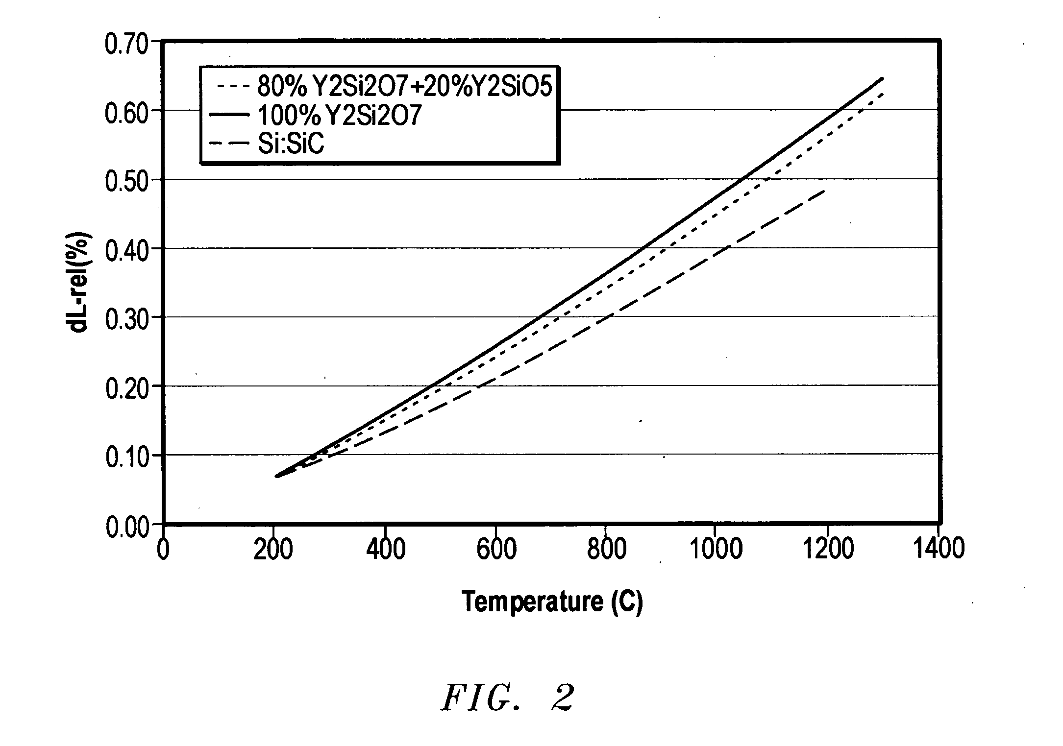
[0042] Coating compositions according to various examples are based on yttrium silicates (Y—Si—O system), particularly two basic mixed metal compositions between SiO2 and Y2O3:Y2Si2O7 and Y2SiO5. The two phases cover a wide thermal expansion coefficient range from 4 ppm / K for Y2Si2O7 to 7 ppm / K for Y2SiO5. The yttrium silicate compounds and blends can be used to protect materials with a wide CTE range, such as from alumina (CTE of ˜8 ppm / K) to SiC (CTE ˜4.5 ppm / K). For example, CTE of Si:SiC can be matched by a 80:20 Y2Si2O7:Y2SiO5 combination as shown in FIG. 2, while the CTE of alumina can be matched by Y2O3 or Y2O3+Y2SiO5 compositions. In addition to Y—Si—O system, rare earth metals such as La, Nd, Gd or Pr can also be used instead of Y due to the relative stability of their respective metal halides.

[0043] Plasma etch tests for Y—Si—O compositions were conducted under two different conditions, fluorine and chlorine plasma tests.

[0044]FIG. 3 compares etch rates of various materi...


PUM

PropertyMeasurementUnit
thicknessaaaaaaaaaa
thicknessaaaaaaaaaa
thicknessesaaaaaaaaaa

Abstract

A semiconductor processing component includes a substrate and a layer overlying the substrate. The layer has a composition ReAyO1.5+2y, wherein Re is Y, La, a Lanthanoid series element, or a combination thereof, A is (Si1−aGea), 0.25≦y≦1.2, and 0≦a≦1.

Description

CROSS-REFERENCE TO RELATED APPLICATION(S) [0001] This application claims priority to both U.S. Provisional Application 60 / 603,984, filed Aug. 24, 2004 and U.S. Provisional Application 60 / 603,985, filed Aug. 24, 2004, the subject matter of both applications thereof being incorporated herein by reference in their entirety.BACKGROUND [0002] 1. Field of the Invention [0003] The present invention is generally directed to semiconductor processing components, and processing techniques utilizing such components. [0004] 2. Description of the Related Art [0005] In modern semiconductor processing, semiconductor wafers are processed through various stations or tools. Processing operations include, for example, high temperature processing such as diffusion, oxidation, ion implant, annealing, and deposition. In each process station or tool, great care is generally taken to minimize contamination of the semiconductor wafers with particles and / or foreign or unwanted species. The demand for ever inc...

Claims


Application Information

Patent Timeline
02 Mar 2006
Publication
US20060046450A1
IPC
H01L21/3205
CPC
C04B35/16; Y10T428/30; C04B2235/3225; C04B2235/3227; C04B2235/3427; C04B2235/80; C04B2235/9607; C04B2235/9692
Inventors
NARENDAR, YESHWANTH; SIMPSON, MATTHEW A.