System and method using locally heated island for integrated circuit testing

Inactive Publication Date: 2006-03-09
IBM CORP
View PDF3 Cites 20 Cited by
  • Summary
  • Abstract
  • Description
  • Claims
  • Application Information

AI Technical Summary

Benefits of technology

[0010] A test system for integrated circuits includes an energy source having an adjustable energy rate, and a feedback device, which measures a physical quantity at a discrete position on an integrated circuit. A control circuit adjusts the power source to

Problems solved by technology

This problem has risen to near crisis levels for high temperature burn-in testing used to accelerate processing faults in CMOS integrated circuits.
This high power at voltages of 1 Volt results in excessive current draw.
These currents exceed the limits of current test equipment.
This method has drawbacks because it forces a voltage island to exist in the chip, and can limit maximum frequency of the chip in normal operation by creating non-uniform voltage regions.
This system is not intended and not suitable for high speed manufacturing burn-in since it relies on a constant current supply instead of a more typical elevated constant voltage supply.
It also has no built in apparatus to allow direct detection of on-chip temperature to control the location of the laser beam.

Method used


Image

  • System and method using locally heated island for integrated circuit testing
  • System and method using locally heated island for integrated circuit testing
  • System and method using locally heated island for integrated circuit testing

Examples


Embodiment Construction

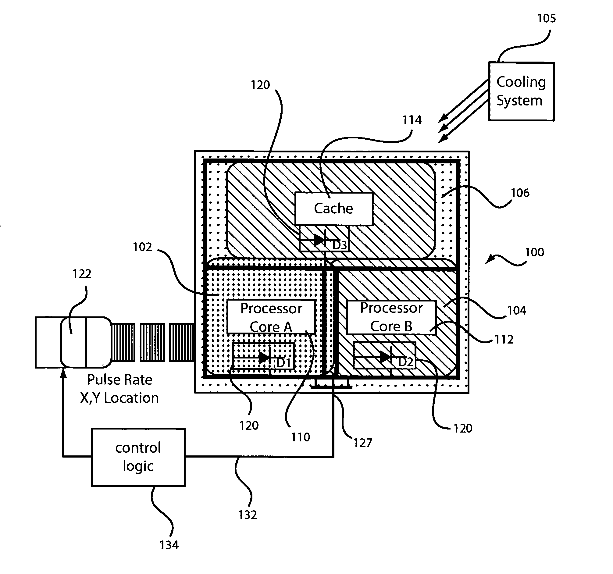
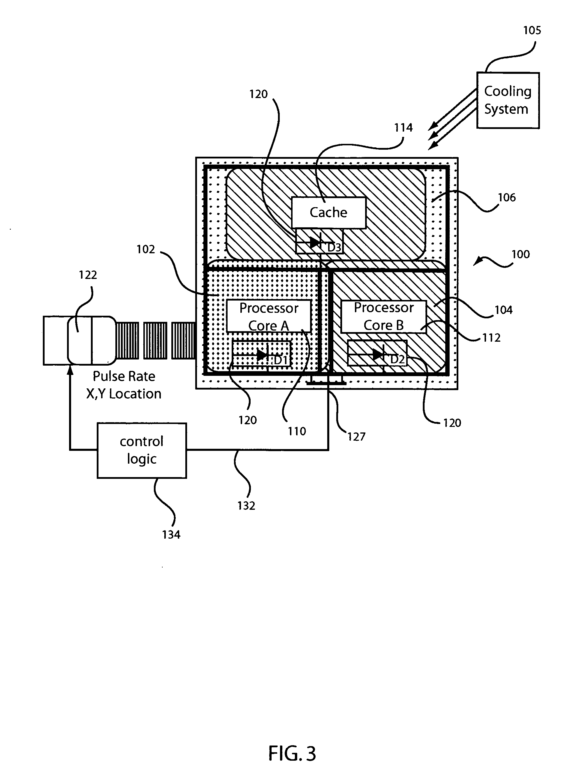
[0019] The present invention employs “thermal islands” within a chip that do not require any voltage supply partitioning in the chip. The thermal island is created by externally heating a location on the chip with a point heat source such as a pulsed high power laser. Integrated thermal circuits, such as diode circuits and control circuits are provided on the chip at key locations. These thermal circuits can be employed with a feedback loop to regulate the laser pulse rate to insure a precise local heating of the chip. This, in turn permits the entire chip to be powered at the same power supply level, while only a portion of the chip is heated to levels that will accelerate thermal faults. After a particular (x1,y1) location is tested, the point source can be electronically repositioned automatically to test another (x2,y2) location of the chip.

[0020] It should be understood that the elements shown in FIGS. may be implemented in various forms of hardware, software or combinations t...


PUM


Abstract

A test system and method for integrated circuits includes an energy source having an adjustable energy rate, and a feedback device, which measures a physical quantity at a discrete position on an integrated circuit. A control circuit adjusts the power source to externally apply energy to the integrated circuit at the discrete position. A circuit tester applies test programs to the integrated circuit while the discrete position is maintained at a value of the physical quantity in accordance with the control circuit.

Description

BACKGROUND OF THE INVENTION [0001] 1. Field of the Invention [0002] The present invention relates to integrated circuit testing, and more particularly to a system and method for controlling temperatures of a chip during testing. [0003] 2. Description of the Related Art [0004] As complementary metal oxide semiconductor (CMOS) technology scales, direct current (D.C.) leakage currents increase dramatically. This problem has risen to near crisis levels for high temperature burn-in testing used to accelerate processing faults in CMOS integrated circuits. Technology scaling has permitted multiple cores to exist on the same chip. Cores may be discrete energy sources and may be associated with parts of a chip (e.g., functional blocks), such as processors, parts thereof or other components, which generate heat. Device leakage at test temperatures in excess of 140° C. can dissipate leakage power in excess of 2000 Watts. This high power at voltages of 1 Volt results in excessive current draw. ...

Claims


Application Information

Patent Timeline
IPC IPC(8): G01R31/26
CPCG01R31/286G01R31/2877G01R31/318533G01R31/31721G01R31/3008
Inventor JENKINS, KEITH A.KOSONOCKY, STEPHEN V.
Owner IBM CORP
Why Eureka
Try Eureka