Incremental erasing of flash memory to improve system performance

Inactive Publication Date: 2006-03-09
TEXAS INSTR INC
View PDF7 Cites 57 Cited by
  • Summary
  • Abstract
  • Description
  • Claims
  • Application Information

AI Technical Summary

Benefits of technology

[0027] It is an object of the invention to reduce the response time to

Problems solved by technology

The un-interrupted 4 or 11 millisecond erase time and resulting CPU idle time is unacceptable in many applications.
This very long wait time may be burdensome or unacceptable to the user.
Furthermore, the foregoing prior art technique causes the time interval allowed for a complete flash memory page erase operation to be very process-dependent.
The wait time required for a flash memory page erase operation represents a very long, often unacceptably long,

Method used


Image

  • Incremental erasing of flash memory to improve system performance
  • Incremental erasing of flash memory to improve system performance
  • Incremental erasing of flash memory to improve system performance

Examples


Example

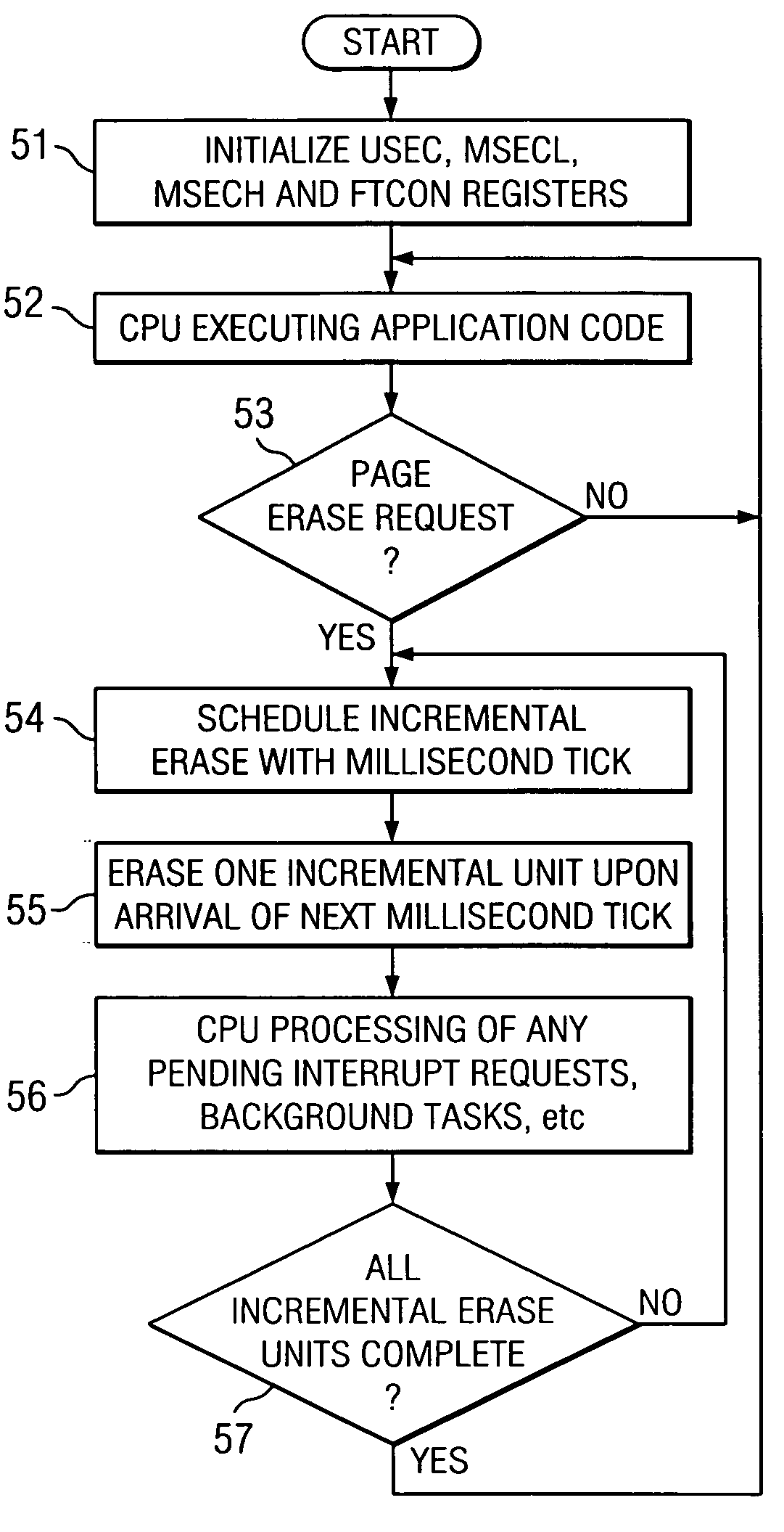
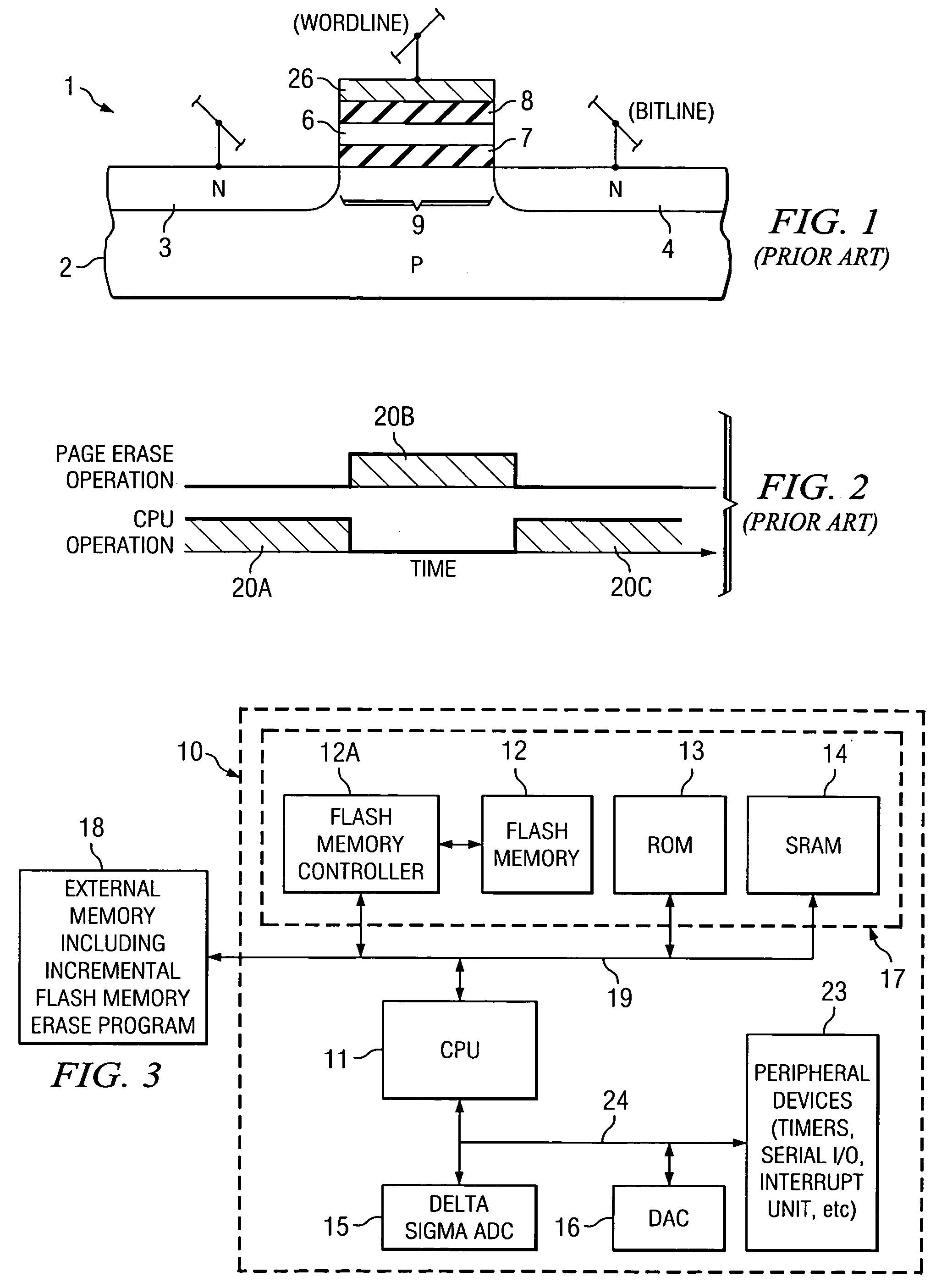
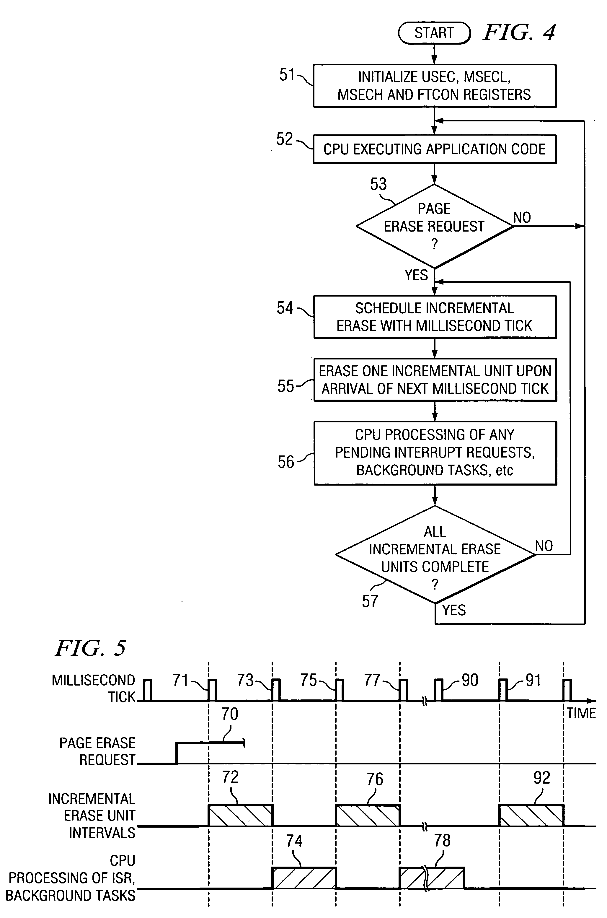
[0041]FIG. 3 is a simplified of diagram of a 24-bit delta sigma ADC microsystem 10 including a microcontroller which includes a CPU, a flash memory cell array, and a flash memory controller. Microsystem 10 also includes an ADC, a DAC, and a number of peripheral devices. Microsystem 10 stores and executes an algorithm which segments flash memory page erase operations to allow faster system response by the CPU to interrupt service routine requests. Microsystem 10 can be the assignee's MSC 1210 microsystem chip.

[0042] Referring to FIG. 3, microsystem 10 is implemented on a single integrated circuit chip, and includes a CPU (central processing unit) 11 coupled to a memory subsystem 17 which includes a static random access memory (SRAM) 14, a read-only memory (ROM) 13, and a TSMC flash memory system including a flash memory array 12 and a flash memory controller 12A, all accessible by CPU 11 via a memory bus 19. The TSMC flash memory system 12,12A can be the TSMC SFA0008—08A8I product w...


PUM


Abstract

A method and system for erasing a page in a flash memory system including a CPU (11), a flash memory (12) including an array of flash memory cells (1), a flash memory controller (12A) coupled to the flash memory (12) and also coupled by a memory bus (19) to the CPU (11) operate the CPU (11) in response to a page erase signal produced during execution by the CPU (11) of a user application program to erase a page of the flash memory by causing the CPU (11) to generate a first incremental erase interval of substantially shorter duration than a total erase time required to erase the flash memory, cause the memory controller (12A) to take control of the memory bus and apply erase signals to the flash memory cells of the page during the first incremental erase interval, and cause the CPU (11) to take control of the memory bus (19) after the first incremental erase interval and execute a pending task. This procedure is repeated for a plurality of additional incremental erase intervals, respectively, the cumulative amount of time of all of the incremental erase intervals being sufficient to result in erasure of the page with a determined retention time.

Description

BACKGROUND OF THE INVENTION [0001] The present invention relates generally to flash memories, and more particularly to a way of reducing system delay in responding to interrupt service routine (ISR) requests and other background tasks during flash memory erase operations. [0002]FIG. 1 shows a section view of a typical flash memory cell, which includes a floating gate MOS structure. Referring to FIG. 1, flash memory cell 1 is formed on a P-type substrate 2 having an N-type source region 3 and an N-type drain region 4 formed in its upper surface. Source region is connected to a conductor used in the erase process. Drain region 4 is connected to a bit line conductor. A channel region 9 within which a N-type channel region can be induced by a “1” voltage level stored on a floating gate 6 is disposed between the edges of source region 3 and drain region 4. A thin gate oxide layer 7 extends over channel region 9. A “floating” gate 6 is a doped, conductive polycrystalline silicon layer for...

Claims


Application Information

Patent Timeline
IPC IPC(8): G06F12/00
CPCG11C2216/22G11C16/16
Inventor CHEUNG, HUGOGHOSH, RITUPARNA
Owner TEXAS INSTR INC
Why Eureka
Try Eureka