Semiconductor device

a semiconductor device and semiconductor technology, applied in the field of misfet, can solve the problems of power loss-generated heat diffusing of semiconductor devices, and achieve the effects of high connection reliability, efficient flow, and large curren

Active Publication Date: 2006-03-16
PANASONIC CORP
View PDF20 Cites 42 Cited by
  • Summary
  • Abstract
  • Description
  • Claims
  • Application Information

AI Technical Summary

Benefits of technology

[0009] An object of the invention is providing a power semiconductor apparatus capable of allowing a large current to efficiently flow and using a wide band gap semiconductor device with high reliability in connection to a mother substrate.

Problems solved by technology

In a power module composed of a plurality of semiconductor chips including a power device, it is conventionally a significant problem to diffuse heat of a semiconductor device generated through power loss of the power device (for example, see Document 1 (Power Electronics Handbook (R & D Planning), edited by Koji Imai (p.

Method used


Image

  • Semiconductor device
  • Semiconductor device
  • Semiconductor device

Examples


embodiment 1

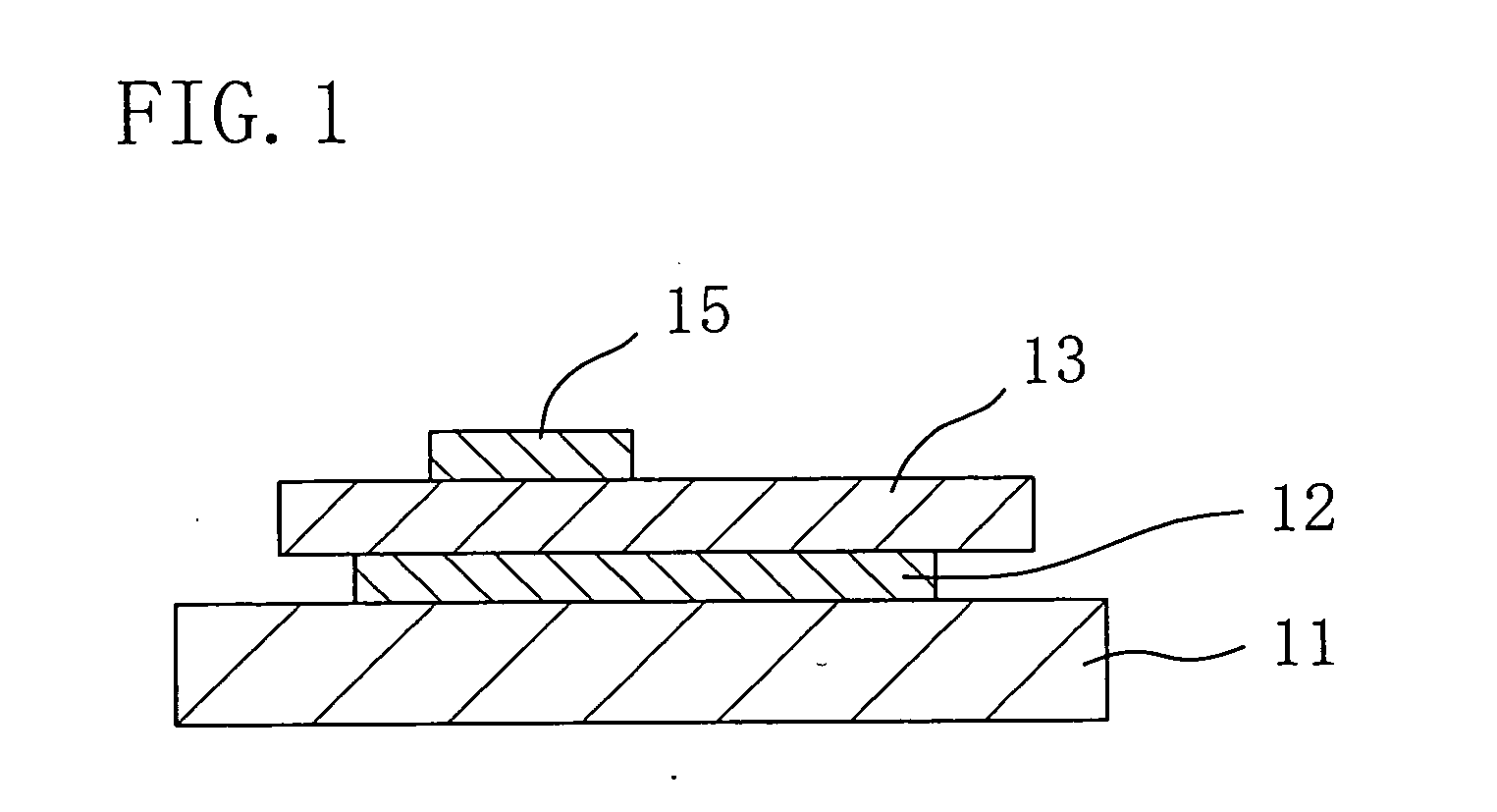
[0036]FIG. 1 is a cross-sectional view for showing the structure of a semiconductor apparatus (power module) according to Embodiment 1 of the invention.

[0037] The semiconductor apparatus (semiconductor power module) according to Embodiment 1 of the invention includes, as shown in FIG. 1, a base material 11 made of a metal material such as Cu and first through third semiconductor chips 12, 13 and 15 (such as a transistor, a diode and an IGBT) different from one another in the size or function and stacked on the base material 11. As characteristics of this semiconductor power module, the semiconductor chips 12, 13 and 15 are stacked with the electrode of at least one semiconductor chip out of the semiconductor chips 12, 13 and 15 connected to the electrode or an active region of another semiconductor chip, and at least one semiconductor chip out of the plural semiconductor chips 12, 13 and 15 includes a semiconductor power device constructed by using a wide band gap semiconductor.

[0...

embodiment 2

[0077]FIGS. 5A and 5B are cross-sectional views for showing two exemplified structures of a semiconductor apparatus according to Embodiment 2 of the invention.

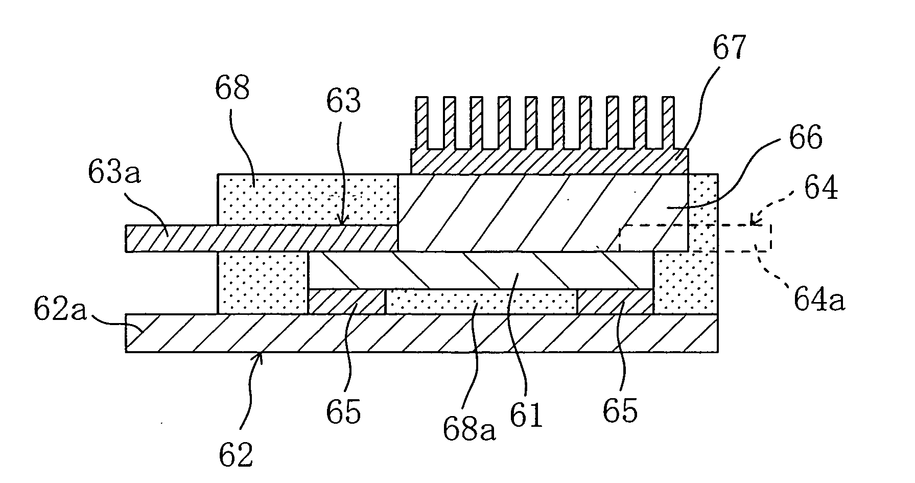
[0078] In the first exemplified structure, as shown in FIG. 5A, the semiconductor apparatus according to Embodiment 2 of the invention includes a semiconductor chip 61 containing a power semiconductor device using a wide band gap semiconductor; a base material 62 corresponding to a die pad made of an electrically conductive metal material such as Cu; a base material 63 corresponding to a lead made of a metal material such Cu and connected to a pad electrode (not shown) of the semiconductor chip 61; a first intermediate member 65 and a second intermediate member 68a disposed between the semiconductor chip 61 and the base material 62 and in contact with a part of the semiconductor chip 61; a heat conducting member 66 in contact with the semiconductor chip 61 and made of a material with high heat conductivity (such as a metal or...

example 1

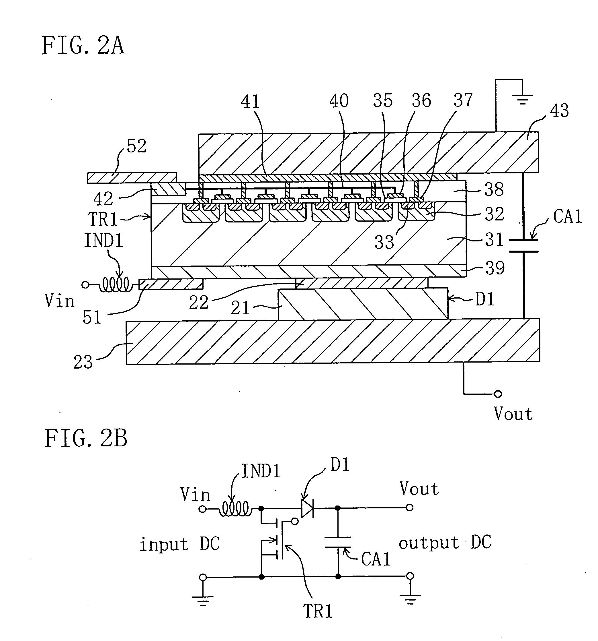
[0099]FIG. 6 is a cross-sectional view of a semiconductor apparatus according to Example 1 of Embodiment 2. As shown in FIG. 6, the semiconductor apparatus of this example includes a power transistor TR1, that is, a vertical MISFET.

[0100] As shown in FIG. 6, the power transistor TR1 (a semiconductor chip 61) includes an N-type drift layer 31 (active region) occupying most of a SiC substrate made of a wide band gap semiconductor; a P-type base layer 32 formed in the N-type drift layer 31 by doping it with a P-type impurity; an N+-type source layer 33 formed in the P-type base layer 32 by doping it with a high concentration N-type impurity; a gate insulating film 35 of a silicon oxide film formed in a surface portion of the SiC substrate over the P-type base layer 32, the N-type drift layer 31 and the N+-type source layers 33 sandwiching the P-type base layer 32; a gate electrode 36 of a metal such as Al or polysilicon provided on the gate insulating film 35; a source electrode 37 fo...


PUM


Abstract

A semiconductor apparatus includes a semiconductor chip 61 including a power semiconductor device using a wide band gap semiconductor, base materials 62 and 63, first and second intermediate members 65 and 68a, a heat conducting member 66, a radiation fin 67, and an encapsulating material 68 for encapsulating the semiconductor chip 61, the first and second intermediate member 65 and 68a and the heat conducting member 66. The tips of the base materials 62 and 63 work respectively as external connection terminals 62a and 63a. The second intermediate member 68a is made of a material with lower heat conductivity than the first intermediate member 65, and a contact area with the semiconductor chip 61 is larger in the second intermediate member 68a than in the first intermediate member.

Description

TECHNICAL FIELD [0001] The present invention relates to a MISFET formed by utilizing a compound semiconductor layer, and more particularly, it relates to a MISFET suitably used for a high breakdown voltage and a large current. BACKGROUND ART [0002] In a power module composed of a plurality of semiconductor chips including a power device, it is conventionally a significant problem to diffuse heat of a semiconductor device generated through power loss of the power device (for example, see Document 1 (Power Electronics Handbook (R & D Planning), edited by Koji Imai (p. 602)). Therefore, a conventional semiconductor apparatus is designed, for cooling a power device and keeping its temperature below the safety operating temperature, to place the power device in contact with the package base material so that heat generated in the power device can be released through a package base material through heat conduction. Accordingly, in the case where a power module is constructed by using a plu...

Claims


Application Information

Patent Timeline
Patent Type & Authority Applications(United States)
IPC IPC(8): H01L23/34H01L23/367H01L23/433
CPCH01L23/3672H01L23/3735H01L2924/13062H01L2924/12032H01L2924/1301H01L2924/10253H01L2924/13055H01L2924/13091H01L24/48H01L2924/19041H01L2924/01079H01L2924/01078H01L2924/0102H01L2924/01004H01L2224/48247H01L23/4334H01L2224/48091H01L2924/00014H01L2924/00H01L2924/12036H01L2924/13063H01L2924/181H01L2924/00012H01L2224/45099H01L2224/45015H01L2924/207H01L23/36
Inventor KITABATAKE, MAKOTOKUSUMOTO, OSAMUUCHIDA, NASAOTAKAHASHI, KUNIMASAYAMASHITA, KENYA
Owner PANASONIC CORP
Why Eureka
Try Eureka