

Photonic interconnections that include optical transmission paths for transmitting optical signals
a technology of optical transmission paths and photonic interconnections, applied in the field of integrated circuit interconnections, can solve the problems of long relative time needed to traverse multiplexed circuit paths, the inability to take full advantage of the high-speed performance of nanoscale components, and the limitations of microscale circuits
- Summary
- Abstract
- Description
- Claims
- Application Information
AI Technical Summary
Benefits of technology
Problems solved by technology
Method used
Image

Examples
Embodiment Construction
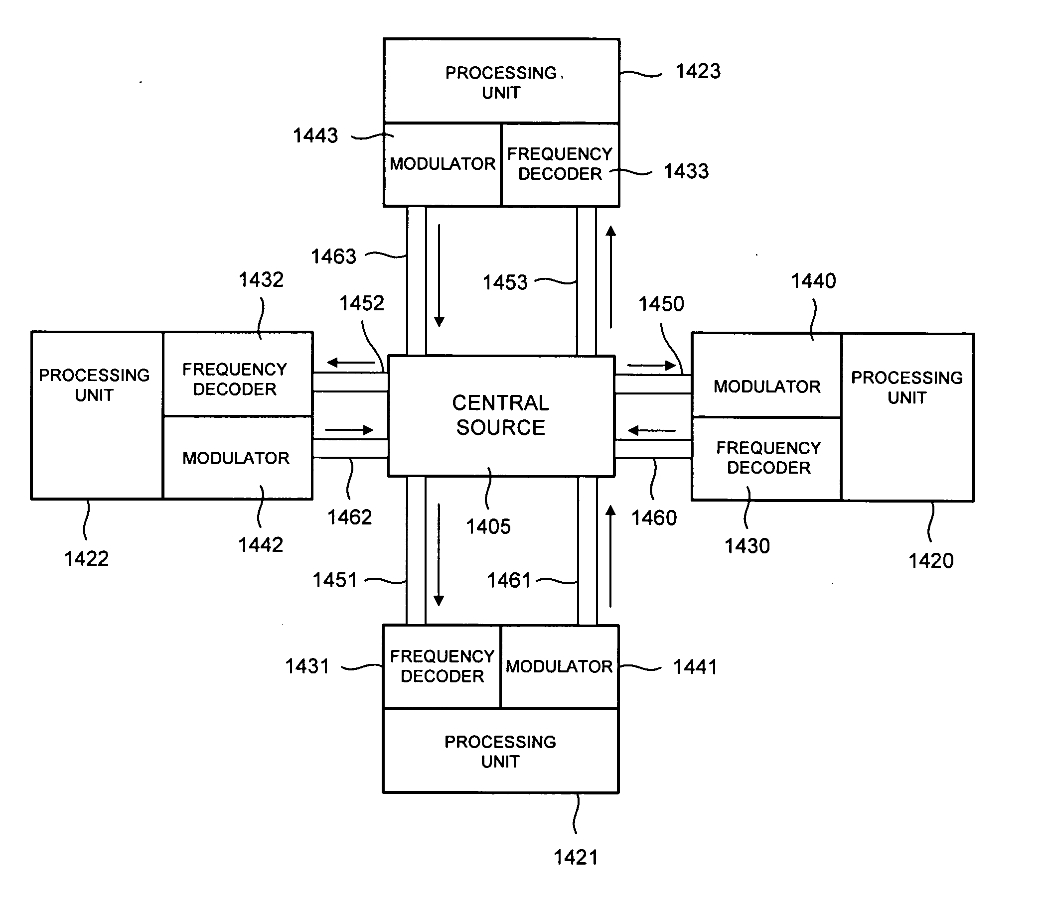
[0072] In one embodiment of the present invention, a large number of relatively high capacitance electrical signal line interconnections needed to transmit address signals, clock signals, and data signals within a computer system are replaced with a relatively small number of high-speed photonic interconnections. In certain embodiments of the present invention, the photonic interconnections are composed of one or more waveguides that confine and direct the transmission of electromagnetic radiation (“ER”). The waveguides can be coaxial cables, optical fibers, line defects in photonic crystals, or any other medium that can be used to simultaneously transmit a number of different frequency channels.
[0073]FIGS. 12A-12C illustrate photonic interconnection architectures for ICs, each representing an embodiment of the present invention. FIG. 12A illustrates a first exemplary IC photonic interconnection architecture. CPU 1200 accesses circuit units 1230-1233 via converter 1220. Circuit uni...
PUM
| Property | Measurement | Unit |
|---|---|---|
| dielectric constant ε2 | aaaaa | aaaaa |
| dielectric constant ε2 | aaaaa | aaaaa |
| dielectric constant | aaaaa | aaaaa |
Abstract
Description
Claims
Application Information