Method and apparatus for receiving high speed signals with low latency

a high-speed signal and low-latency technology, applied in the field of high-speed signal receiving methods and apparatuses, can solve the problems of amplifiers b>186/b> consuming static direct current and static power, limited input common-mode range, and low voltage gain of integrators b>182/b>

Inactive Publication Date: 2006-03-23
RAMBUS INC
View PDF99 Cites 34 Cited by
  • Summary
  • Abstract
  • Description
  • Claims
  • Application Information

AI Technical Summary

Benefits of technology

[0002] The present invention relates generally to a high frequency digital signal receiver, and more particularly to a digital signal receiver that uses integration techniques to reduce latency of signals on a bus.

Problems solved by technology

One disadvantage of this integrator 182 is that its input common-mode range is limited.
Another disadvantage is that the integrator 182 has a low voltage gain when either transistor 206 or 208 of the differential pair does not fully steer the current IBIAS to either of the integration nodes NINTA and NINTB.
However, supplying the amplifier bias current IBIASA in this way causes the amplifier 186 to consume static direct current and therefore static power.
Because the amplifier 186 consumes a significant amount of static power, the amplifier 186 may be unsuitable for use in devices that use a large number of receivers.
Therefore, the input-to-output latency consumes a significant portion of the system clock period.
In particular, the input-to-output latency consumes a large amount of time relative to a typical clock cycle time of approximately two nanoseconds (ns) for high speed signaling systems, and potentially limits the performance of the system in which the integrating receiver is used.

Method used


Image

  • Method and apparatus for receiving high speed signals with low latency
  • Method and apparatus for receiving high speed signals with low latency
  • Method and apparatus for receiving high speed signals with low latency

Examples


Embodiment Construction

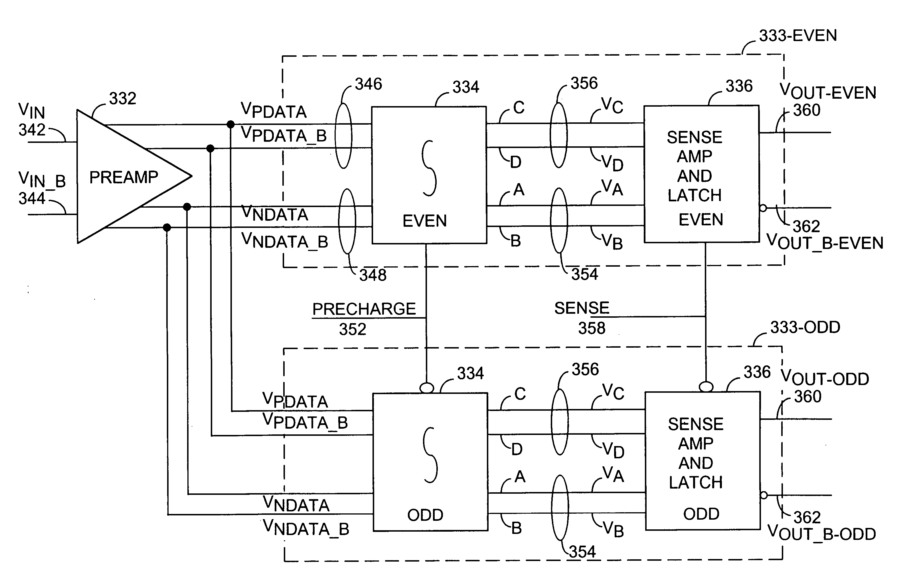
[0118] In FIG. 6, a bus 320 interconnects a memory controller 321 and memories 322. The bus 320 is formed of signal lines 320-1, 320-2 that transmit address, data and control signals. Physically, on each integrated circuit 321, 322, the address, data and control signals are supplied to and output from external connections, called pins, and the bus 320 interconnects respective pins. The bus 320 may be implemented as traces on a printed circuit board, wires or cables and connectors. Each of these integrated circuits 321, 322 has bus output driver circuits 323 that connect to the pins to interface with the bus 320 to transmit signals to other ones of the integrated circuits. In particular, the bus output drivers 323 in the memory controller 321 and in the memories 322 transmit data over the bus 320. Each bus output driver 323 drives a single signal line of the bus 320. For example, bus output driver 323-1 in the memory controller 321 drives bus line 320-1. The bus 320 supports signalin...


PUM


Abstract

An apparatus and method for receiving high-speed signals having a wide common-mode range with low input-to-output latency. In one embodiment, the receiver includes an integrator to accumulate charge in accordance with an input signal during an integration time interval to produce an output voltage. A sense amplifier samples and converts the output voltage of the integrator to a logic signal; and a latch stores the logic signal. In an alternate embodiment, a preamplifier conditions the input signal prior to being integrated. In another embodiment using multiple receivers, circuitry is added to the receiver to compensate for timing errors associated with the distribution of the timing signals. In yet another embodiment, the integrator is coupled to an equalization circuit that compensates for intersymbol interference. In another embodiment, another circuit compensates for accumulated voltage offset errors in the integrator.

Description

CROSS REFERENCE TO RELATED APPLICATIONS [0001] This application is a continuation of application Ser. No. 10 / 123,370 filed on Apr. 15, 2002; which is a divisional of application Ser. No. 09 / 478,914, filed Jan. 6, 2000, now U.S. Pat. No. 6,396,329; which claims priority to provisional patent application 60 / 158,189, filed Oct. 19, 1999, each of which is hereby incorporated by reference for all purposes.BRIEF DESCRIPTION OF THE INVENTION [0002] The present invention relates generally to a high frequency digital signal receiver, and more particularly to a digital signal receiver that uses integration techniques to reduce latency of signals on a bus. BACKGROUND OF THE INVENTION [0003] An efficient high speed signaling system requires the use of well-controlled waveforms. For example, in a high speed signaling system with a clock cycle time in the range of approximately one to two nanoseconds, the amplitude of the voltage swing, the rise and fall times, and the duty cycle of the signaling...

Claims


Application Information

Patent Timeline
Patent Type & Authority Applications(United States)
IPC IPC(8): G06G7/18G11C7/10H04L7/033H04L25/02H04L25/03
CPCG11C7/02H03K5/133G11C7/1057G11C7/106G11C7/1078G11C7/1084G11C7/1087G11C7/1096G11C7/22G11C7/222G11C8/10H03K3/356034H03K5/131H03K17/162H03K19/00323H03K19/018528H03K2005/00065H03M5/20H04L7/0332H04L25/0276H04L25/028H04L25/0292H04L25/03878G11C7/1051
Inventor ZERBE, JARED L.
Owner RAMBUS INC
Why Eureka
Try Eureka