Semiconductor device comprising light-emitting element and light-receiving element, and manufacturing method therefor

a technology of light-emitting elements and semiconductor devices, which is applied in the direction of basic electric elements, color television, television systems, etc., can solve the problems of increasing the thickness of the packaged semiconductor device, difficult to achieve a reduction in size, and the packaging method using ceramic headers is also problematic, so as to prevent short circuiting of the wiring pattern due to external shocks and the like, reduce the size, and reduce the effect of siz

Inactive Publication Date: 2006-03-30
LAPIS SEMICON CO LTD
View PDF5 Cites 47 Cited by
  • Summary
  • Abstract
  • Description
  • Claims
  • Application Information

AI Technical Summary

Benefits of technology

[0014] According to the present invention, there is no need to mount the semiconductor device on a ceramic header, as is performed conventionally, and hence the final, packaged form of the semiconductor device can be reduced in size.
[0015] Also according to the present invention, the side portion of the columnar electrode is coated in resin, and hence short circuiting of the wiring patterns due to external shocks and the like can be prevented. Furthermore, disconnection of the wiring patterns caused when the device contacts the wiring patterns during handling of the semiconductor device package can also be prevented.
[0016] Also according to the present invention, the cut surface formed by dicing is constituted by only two layers, i.e. a single sealant and a transparent substrate, having no boundary lines between resin layers, and hence problems such as breakage of the resin during a heating process such as reflow processing can be reduced. Furthermore, moisture or the like is prevented from infiltrating through the boundary lines of the resin layers, and hence the long-term reliability of the wiring and the semiconductor chip can be improved.
[0017] According to the manufacturing method of the present invention, the manufacture of a semiconductor device comprising a light-receiving element or a light-emitting element can be realized at the wafer level, and hence the size and cost of the manufactured device can be reduced. Moreover, a manufacturing method in which layers are formed in succession on the transparent substrate is employed, and hence there is no need to adhere the transparent substrate and semiconductor wafer together. As a result, alignment errors are eliminated, enabling an improvement in productivity.

Problems solved by technology

Moreover, space must be provided above the semiconductor chip for the wire bonding and lid, thereby increasing the thickness of the packaged semiconductor device, and hence it is difficult to achieve a reduction in size.
Packaging methods using a ceramic header are also problematic in that costs are higher than in packaging methods using resin.
Moreover, during handling of the individual packages, the electrode pattern may become disconnected when the electrode pattern contacts a semiconductor holder used for lifting the semiconductor device.
Also with the manufacturing method of the patent document-1, the wafer comprising the light-receiving element and the translucent substrate comprising the lens are formed separately and then adhered together, leading to alignment errors which result in a decrease in productivity.
In the patent document-2, the side face of the semiconductor device is constituted by a sealant using a plurality of resin layers, and hence cracks or the like may appear at the boundary line parts of these resin layers during a heating process such as reflow processing, possibly causing the semiconductor device to break.
Further problems such as corrosion of the wiring layers formed in the semiconductor device due to moisture infiltrating through the boundary lines of the resin layers, and abnormalities in the characteristics of the semiconductor element due to the incoming moisture, may lead to a breakdown in the functions of the semiconductor element, resulting in a reduction in the long-term reliability of the device.

Method used


Image

  • Semiconductor device comprising light-emitting element and light-receiving element, and manufacturing method therefor
  • Semiconductor device comprising light-emitting element and light-receiving element, and manufacturing method therefor
  • Semiconductor device comprising light-emitting element and light-receiving element, and manufacturing method therefor

Examples


second embodiment

[0087] [Structure]

[0088] The structure of a semiconductor device according to a second embodiment of the present invention will now be described using FIGS. 11 and 12.

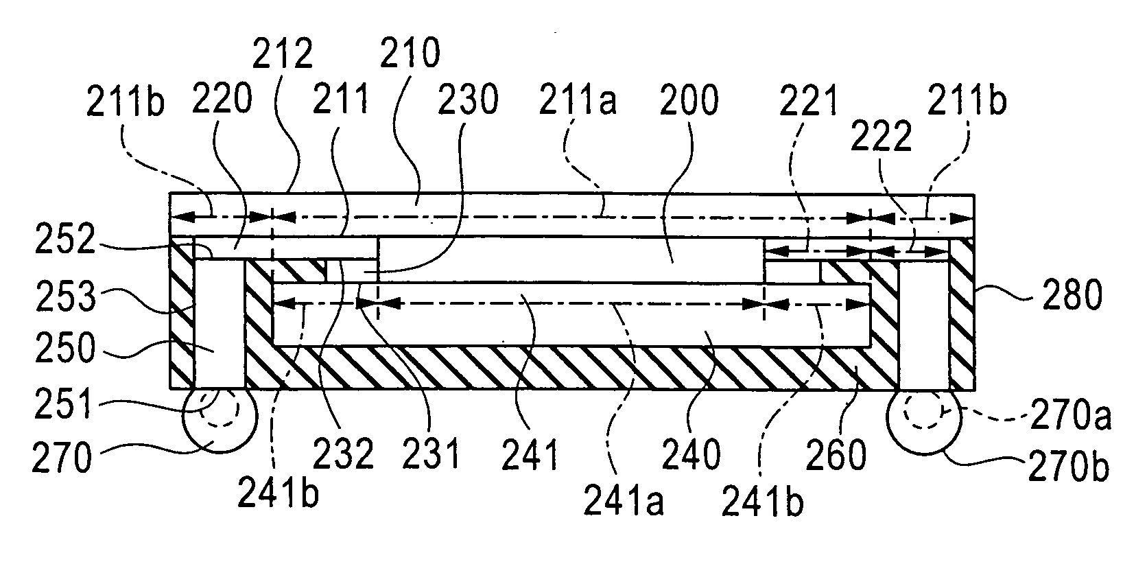
[0089]FIG. 11 is a plan view of the semiconductor device according to the second embodiment of the present invention, and FIG. 12 is a sectional view along A-A in FIG. 11.

[0090] As shown in FIGS. 11 and 12, the semiconductor device according to the second embodiment of the present invention includes a transparent substrate 1210, a wiring layer 1220, a bump electrode 1230, a semiconductor chip 1240, a columnar electrode 1250, a sealant 1260, an external connection terminal 1270, a lens portion 1280, and a cut surface 1290. Detailed description of constitutional parts that are identical to the first embodiment has been omitted.

[0091] The transparent substrate 1210 comprises a rectangular first face 1211 having a first central region 1211a and a first peripheral region 1211b surrounding the first central region 1211a, ...

third embodiment

[0108] [Structure]

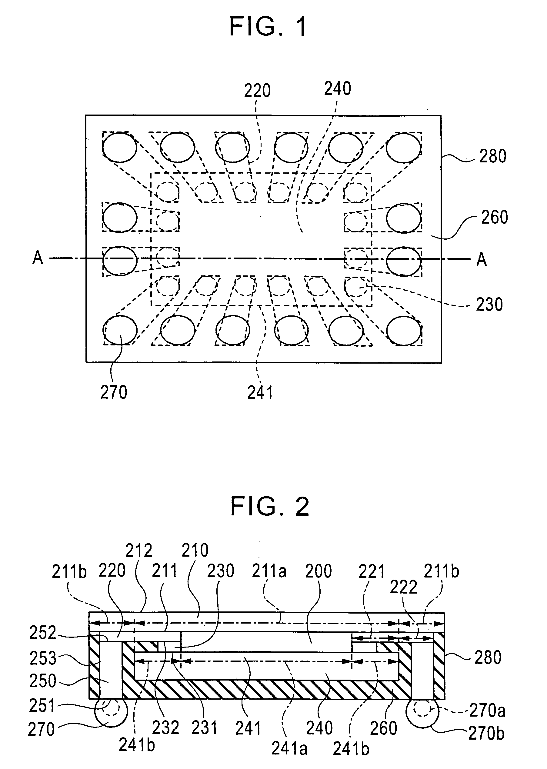
[0109] The structure of a semiconductor device according to a third embodiment of the present invention will now be described using FIGS. 19 and 20.

[0110]FIG. 19 is a plan view of the semiconductor device according to the third embodiment of the present invention, and FIG. 20 is a sectional view along A-A in FIG. 19.

[0111] As shown in FIGS. 19 and 20, the semiconductor device according to the third embodiment of the present invention includes a transparent substrate 2010, a wiring layer 2020, a bump electrode 2030, a semiconductor chip 2040, a columnar electrode 2050, a sealant 2060, an external connection terminal 2070, a lens portion 2080 formed on the transparent substrate 2010, and a cut surface 2090. Detailed description of constitutional parts that are identical to the first embodiment has been omitted.

[0112] The transparent substrate 2010 comprises a rectangular first face 2011 having a central region 2011a and a peripheral region 2011b surrounding the ce...

fourth embodiment

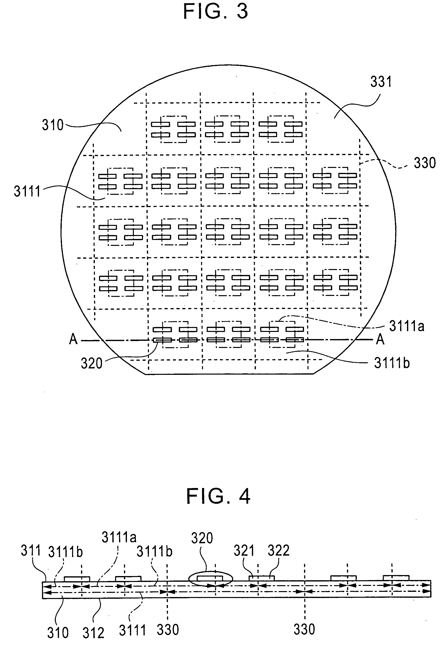
[0122] The structure of a semiconductor device according to a fourth embodiment of the present invention will now be described using FIGS. 25 and 26.

[0123]FIG. 25 is a plan view of the semiconductor device according to the fourth embodiment of the present invention, and FIG. 26 is a sectional view along A-A in FIG. 25.

[0124] As shown in FIGS. 25 and 26, the semiconductor device according to the fourth embodiment of the present invention includes a transparent substrate 2610, a first wiring layer 2620, a second wiring layer 2621, a third wiring layer 2622, a first bump electrode 2630, a second bump electrode 2631, a third bump electrode 2632, a fourth bump electrode 2633, a first semiconductor chip 2640, a second semiconductor chip 2650, a first columnar electrode 2660, a second columnar electrode 2670, a sealant 2680, a first external connection terminal 2690, a second external connection terminal 2691, and a cut surface 2510.

[0125] The transparent substrate 2610 comprises a rect...


PUM


Abstract

A semiconductor device includes a substrate for transmitting light, a wiring layer provided on the substrate, a semiconductor chip formed on the wiring layer, a columnar electrode, a sealant, and an external connection terminal electrically connected to the semiconductor chip via the wiring layer and protruding electrode. The device includes a cut surface formed by dicing and constituted by only the substrate and the sealant. Since the cut surface has a single-layer structure as a result of forming the sealant in a single step, moisture cannot infiltrate through the sealant, hence a device resistant to corrosion and operational defects is provided.

Description

BACKGROUND OF THE INVENTION [0001] 1. Field of the Invention [0002] The present invention relates principally to a semiconductor device and a packaging method thereof, and more particularly to a semiconductor device comprising a light-receiving element which operates in response to light and a light-emitting element which emits light, for example a semiconductor device including an image sensor such as a CCD or CMOS, a light-emitting diode, a photoelectric conversion element, and so on, and a packaging method thereof. [0003] 2. Description of the Related Art [0004] Conventionally, when packaging a semiconductor device comprising a light-receiving element and light-emitting element manufactured in wafer form, the wafer on which the light-receiving elements and / or light-emitting elements are formed is cut into individual semiconductor chips 4410 by means of dicing, as shown in FIG. 44. The individual semiconductor chip 4410 is then mounted on a ceramic header 4420, whereupon an electr...

Claims


Application Information

Patent Timeline
Patent Type & Authority Applications(United States)
IPC IPC(8): H01L23/48H01L23/02H01L27/14H01L31/02H01L33/48H01L33/54H01L33/56H01L33/62H04N5/335H04N5/369H04N5/372H04N5/374
CPCH01L21/56H01L2924/15192H01L24/97H01L27/14618H01L27/14625H01L27/14683H01L27/14685H01L31/0203H01L31/0232H01L2224/16H01L2224/48091H01L2224/97H01L2924/01018H01L2924/01029H01L2924/01047H01L2924/01049H01L2924/01074H01L2924/01078H01L2924/01079H01L2924/01082H01L2924/10329H01L2924/1532H01L23/3128H01L2924/12041H01L2224/48227H01L2924/01033H01L24/48H01L2924/01005H01L2924/01006H01L2924/00014H01L2224/81H01L31/02325H01L2924/00011H01L2924/15788H01L2924/16195H01L2924/00H01L2224/0401H01L2224/45099H01L2224/45015H01L2924/207
Inventor OHSUMI, TAKASHI
Owner LAPIS SEMICON CO LTD
Why Eureka
Try Eureka