Solid state image pickup element and method of manufacturing solid state image pickup element

a technology of solid state image and pickup element, which is applied in the direction of television system, radio frequency control device, instruments, etc., can solve the problems of void where no color filter is formed, fluctuation in size and shape, and fluctuation in production fluctuation of recent solid state image pickup element, so as to reduce the characteristic distribution of in-plane photoelectric conversion portion and reduce image non-uniformity

Inactive Publication Date: 2006-04-13
CANON KK
View PDF6 Cites 11 Cited by
  • Summary
  • Abstract
  • Description
  • Claims
  • Application Information

AI Technical Summary

Benefits of technology

[0030] The present invention has been made to solve the above-described problems of prior art, and an object of the present invention is therefore to provide a solid state image pickup element manufacturing method and a solid state image pickup element which can exponentially reduce the in-plane photoelectric conversion portion characteristic distribution that is created in forming color filters by a common photolithography technique and which, when color filters are formed by split exposure, can reduce image non-uniformity between exposure regions in a picked-up image.

Problems solved by technology

Recent solid state image pickup elements suffer from various kinds of production fluctuation (such as mask size differences, microlens distortion components, exposure light distribution in one shot, mask alignment precision, and changes with time of resist characteristics) due to the increased level of pixel integration.
Such production fluctuation causes fluctuation in size and shape of color filters or mispositioning of color filters, with the result that adjacent color filters overlap each other or a void is created between adjacent color filters.
In the solid state image pickup element manufacturing method described above, corners of the color filters are rounded because of lowering of the resolution of the exposure device, and a void where no color filters are formed is also created in such corners.
This means that a pixel signal outputted contains a shading component and a color mixture component corresponding to the void width and the overlapping amount, thereby causing degradation of a picked-up image.
Therefore, it is very difficult to give color filters of different exposure regions the same size as well as to align a color filter of one exposure region identically to a color filter of another exposure region.
Furthermore, overlapping of adjacent color filters and a void between adjacent color filters give the second planarization film formed on the color filters insufficient levelness, and surface irregularities are created in the second planarization film above the color filter overlapping portion and the color filter void portion.
As a result, dispersed light reaches the photoelectric conversion portion through color filters and causes fluctuation in amount of incident light among pixels.
In the color filter overlapping portion, on the other hand, light passes through the combined thicknesses of two color filters and is attenuated in the process before reaching the photoelectric conversion portion, resulting in fluctuation in amount of incident light among pixels.
As a result, when a solid state image pickup element formed by the split exposure method is used in picking up an image, visible streaks of image non-uniformity are found in portions of the picked-up image that correspond to interfaces between divided exposure regions.
However, it is impossible to reduce process fluctuation in an exposure region, namely, in-plane distribution, to nil.
In addition, exposure process differences between exposure regions cannot be eradicated as long as the split exposure method above is employed.
It has therefore been difficult in prior art to restrain within a certain range the difference in light detection sensitivity between exposure regions.

Method used


Image

  • Solid state image pickup element and method of manufacturing solid state image pickup element
  • Solid state image pickup element and method of manufacturing solid state image pickup element
  • Solid state image pickup element and method of manufacturing solid state image pickup element

Examples


first embodiment

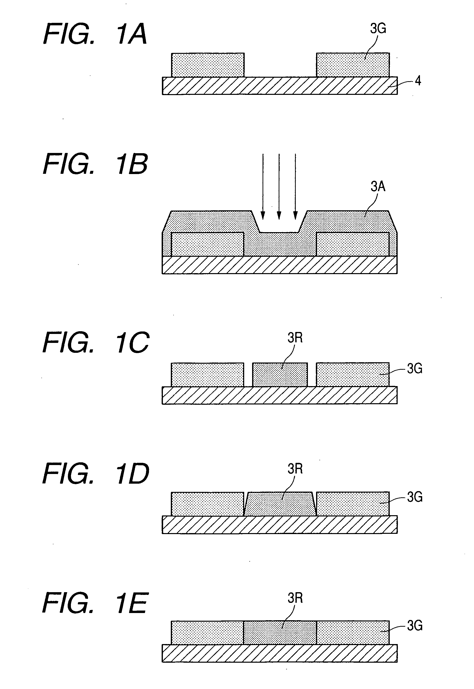
[0052]FIGS. 1A to 1E are sectional views showing a manufacture procedure in a first embodiment of a solid state image pickup element of the present invention.

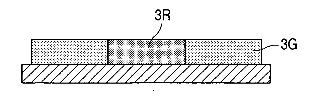
[0053] The solid state image pickup element shown in FIGS. 1A to 1E has a pixel pitch of 9 μm and color filters are arranged in accordance with the Bayer pattern similar to the conventional solid state image pickup elements shown in FIGS. 12 and 13. The structure of this solid state image pickup element is identical with that of the conventional solid state image pickup element shown in FIG. 8 except the shapes of the color filters, and therefore a description of the identical part is omitted here.

[0054] In a solid state image pickup element manufacturing method of this embodiment, the first step is to apply negative color resist with, for example, a green (G) pigment dispersed therein to a surface of a first planarization film 4 as shown in FIG. 1A. Then a mask which blocks light except where G filters are to be formed is pl...

second embodiment

[0062]FIGS. 3A to 3E are sectional views showing a manufacture procedure in a second embodiment of a solid state image pickup element of the present invention.

[0063] The solid state image pickup element shown in FIGS. 3A to 3E, similarly to the first embodiment, has a pixel pitch of 9 μm and color filters are arranged in accordance with the Bayer pattern.

[0064] In a solid state image pickup element manufacturing method of the second embodiment, the first step is to apply negative color resist with, for example, a green (G) pigment dispersed therein to a surface of a first planarization film 4 as shown in FIG. 3A. Then a mask which blocks light except where G filters 13G are to be formed is placed for irradiation with ultraviolet rays having a wavelength of, for example, 365 nm, and for subsequent development. Thus G filters 13G are formed on the first planarization film 4.

[0065] In this embodiment, the G filters 13G are exposed to light through ultraviolet irradiation of varying ...

third embodiment

[0074]FIGS. 6A to 6E are sectional views showing a manufacture procedure in a third embodiment of a solid state image pickup element of the present invention.

[0075] The solid state image pickup element shown in FIGS. 6A to 6E, similarly to the first embodiment, has a pixel pitch of 9 μm and color filters are arranged in accordance with the Bayer pattern.

[0076] In a solid state image pickup element manufacturing method of the third embodiment, similarly to the first embodiment, the first step is to apply negative color resist with, for example, a green (G) pigment dispersed therein to a surface of a first planarization film 4. Then a mask which blocks light except where G filters 23G are to be formed is placed for irradiation with ultraviolet rays having a wavelength of, for example, 365 nm, and for subsequent development. Thus G filters 23G are formed on the first planarization film 4 as shown in FIG. 6A. In this embodiment, the G filters 23G are exposed to light through ultraviol...


PUM

PropertyMeasurementUnit
wavelengthaaaaaaaaaa
widthaaaaaaaaaa
widthaaaaaaaaaa

Abstract

Provided is a solid state image pickup element which can exponentially reduce the in-plane photoelectric conversion portion characteristic distribution that is created in forming color filters by a common photolithography technique and which, when color filters are formed by split exposure, can reduce image non-uniformity between exposure regions in a picked-up image, and a method of manufacturing the same. The method includes: applying negative type color resist for forming first color filters onto an entire surface of a given film; forming the first color filters by irradiation of given portions with exposure light and by subsequent development; applying negative type color resist for forming second color filters onto the entire surface of the first color filters while covering the first color filters; and forming the second color filters by irradiating an area smaller than a region that is surrounded by the first color filters with exposure light and by subsequent development. Further, in the solid state image pickup element with color filters of plural colors, one of adjacent color filters is tapered at the edges while the other color filter is reversely tapered at the edges, allowing the adjacent color filters to fit to each other. Furthermore, adjacent color filters are wedged at the edges, allowing the adjacent color filters to fit to each other.

Description

BACKGROUND OF THE INVENTION [0001] 1. Field of the Invention [0002] The present invention relates to a solid state image pickup element having a color filter for picking up a color image, and to a method of manufacturing a solid state image pickup element. [0003] 2. Related Background Art [0004]FIG. 8 shows one of the structures, which have been known, as solid state image pickup elements, for use in color video cameras and color still cameras. [0005]FIG. 8 is a side sectional view showing the structure of a conventional solid state image pickup element. [0006] The solid state image pickup element shown in FIG. 8 has, in the vicinity of a surface of a semiconductor substrate 100, a photoelectric conversion portion 110 which generates signal charges according to the amount of incident light. The photoelectric conversion portion 110 is provided in each of pixels that are arranged to form a lattice pattern. [0007] The pixels each have a driver circuit for generating a pixel signal in a...

Claims


Application Information

Patent Timeline
Patent Type & Authority Applications(United States)
IPC IPC(8): H01L31/062H01L21/00G03F7/004G02B5/20G03F7/20H01L21/027H01L27/14H01L27/146H01L31/00H01L31/0216H04N5/335H04N5/369
CPCH01L27/14621H01L27/14623H01L27/14627H01L27/14685H01L31/02162
Inventor SEKINE, YASUHIROMORI, SHIGEKI
Owner CANON KK
Why Eureka
Try Eureka