Method for flip chip package and structure thereof

a chip and package technology, applied in the field of flip chip packages, can solve the problems of reducing the reliability of the chip, increasing the heat dissipation of the chip, and increasing the cost of the chip, and achieve the effect of enhancing the thermal dissipation capability and high thermal conductivity

Inactive Publication Date: 2006-04-13
VIA TECH INC
View PDF7 Cites 25 Cited by
  • Summary
  • Abstract
  • Description
  • Claims
  • Application Information

AI Technical Summary

Benefits of technology

[0020] As mentioned above, by using the eutectic bonding process to form a gold-silicon intermetallic layer with high thermal conductivity between a chip and a heatsink, the present invention enhances thermal dissipation capability from the chip to the heatsink and ensuring the chip working well.

Problems solved by technology

However, accompanying to the progress of functionality of integrated circuit, the chip dissipates much more heat during operation.
In order to prevent the reduction of reliability of the chip caused by dissipated heat, heat dissipation has become a major issue, especially to the products of high power consumption such as central processing unit (CPU) and graphics processing unit (GPU).
In prior art, the most popular TIM on CPU is thermal grease or phase change material, such as epoxy based material or tin-lead solder, the resistivity is too high to get a good result.
The thermal conductivity of epoxy based TIM is too low to have a good thermal dissipation capability.

Method used


Image

  • Method for flip chip package and structure thereof
  • Method for flip chip package and structure thereof
  • Method for flip chip package and structure thereof

Examples


Embodiment Construction

[0029] The present invention will be apparent from the following detailed description, which proceeds with reference to the accompanying drawings, wherein the same references relate to the same elements.

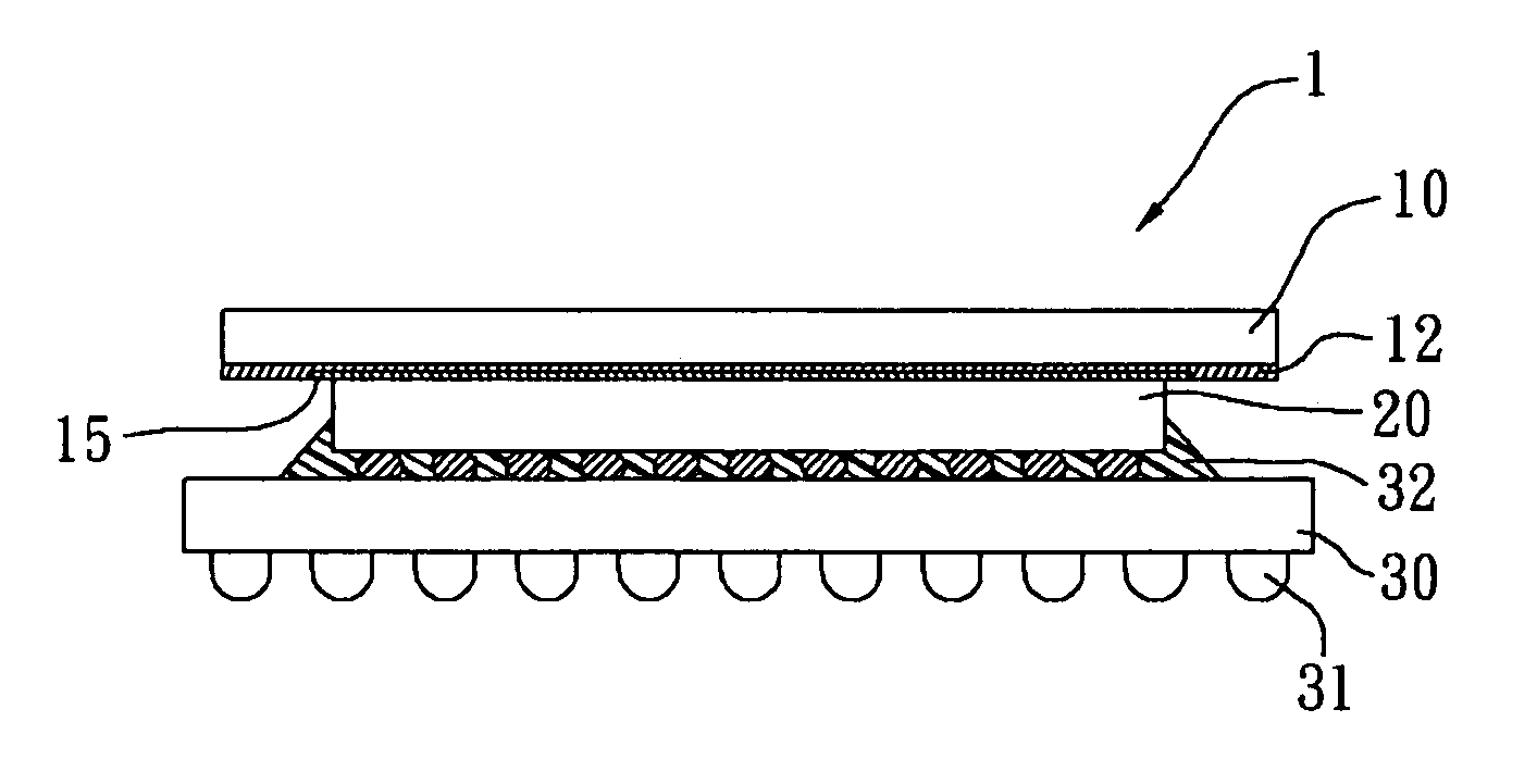
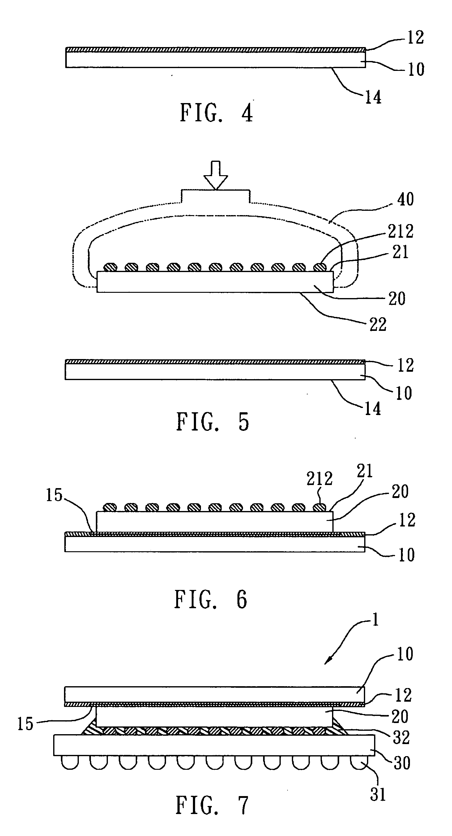
[0030] FIGS. 4 to 7 show a method for a flip chip package according to the present invention. As shown in FIG. 4, a heatsink 10 having a surface plated with a gold film 12 and a bare surface 14 is provided.

[0031] As shown in FIG. 5, a chip 20 having a join surface 22 and an active surface 21 with a plurality of contacts 212 is provided. Then, a clamping apparatus 40 to clamp the chip 20 and to dispose the join surface 22 of the chip 20 onto the gold film 12 of the heatsink 10.

[0032] As shown in FIG. 6, the join surface 22 of the chip 20 is connected to the gold film 12 of the heatsink 10 by an eutectic bonding process. Due to the chip 20 is made of silicon, eutectic reaction between gold and silicon at about 363° C. will form a gold-silicon intermetallic layer by gold-silicon diff...


PUM


Abstract

A method for flip chip package and structure thereof is disclosed. The present invention is using an eutectic bonding process to connect a chip and a heatsink for enhancing thermal dissipation capability from the chip to the heatsink and ensuring the chip working well. The method for flip chip package at least includes the steps of providing a heatsink having a surface plated with a gold film and a bare surface, providing a chip having a join surface and an active surface with a plurality of contacts, eutectic bonding the join surface of the chip to the gold film of the heatsink by gold-silicon diffusion for connecting the chip to the heatsink, connecting the active surface of the chip to a substrate by flip chip technology; and dispensing an underfill into the gap between the chip and the substrate.

Description

BACKGROUND OF THE INVENTION [0001] 1. Field of Invention [0002] The present invention relates to a flip chip package, and in particular, to a method for flip chip package and structure thereof by connecting a chip with a heatsink by using an eutectic bonding process. [0003] 2. Related Art [0004] Flip chip package has been widespread applied to semiconductor package. Comparing to prior wire bonding ball grid array (WBBGA), flip chip package reverses a chip and mechanically and electrically connects an active surface (the surface with electronic circuit and devices) of the chip to a substrate by plural solder bumps. An insulating underfill is then dispensed into the gap between the solder bumps and between the chip and the substrate for solid connection. Because no wire is needed for electrical connection, flip chip package can reduce the packaging size and be more compact. [0005] However, accompanying to the progress of functionality of integrated circuit, the chip dissipates much mo...

Claims


Application Information

Patent Timeline
Patent Type & Authority Applications(United States)
IPC IPC(8): H01L21/48
CPCH01L21/4875H01L21/563H01L2224/73203H01L2924/01079H01L2924/01322H01L2924/01327H01L2924/00
Inventor YANG, CHIH-AN
Owner VIA TECH INC
Why Eureka
Try Eureka