Film circuit substrate having Sn-In alloy layer

Inactive Publication Date: 2006-05-04
SAMSUNG ELECTRONICS CO LTD
View PDF12 Cites 13 Cited by
  • Summary
  • Abstract
  • Description
  • Claims
  • Application Information

AI Technical Summary

Benefits of technology

[0020] In one embodiment, a film circuit substrate comprises an insulating film made of polyimide resin; a conductive circuit pattern formed on the insulating film, the circuit pattern including an inner lead to be connected with a conductive bump of a semiconductor chip through a bump bonding process; and a tin-indium alloy layer formed on the inner lead to produce an inter-metall

Problems solved by technology

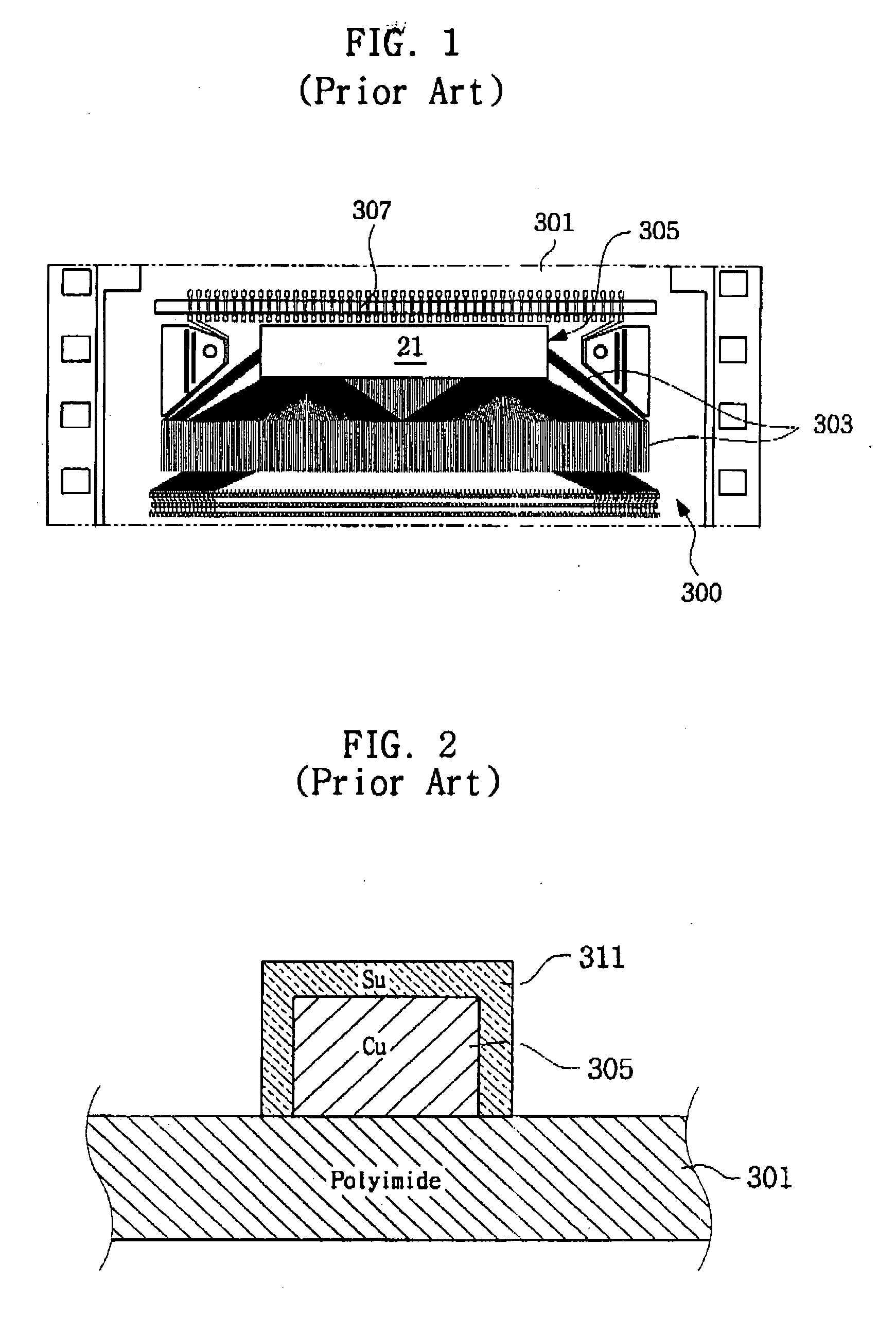
In liquid crystal display (LCD) panel markets, the demand for driver integrated circuit chips to support colors and moving pictures has caused an explosive increase in the number of chip pads.
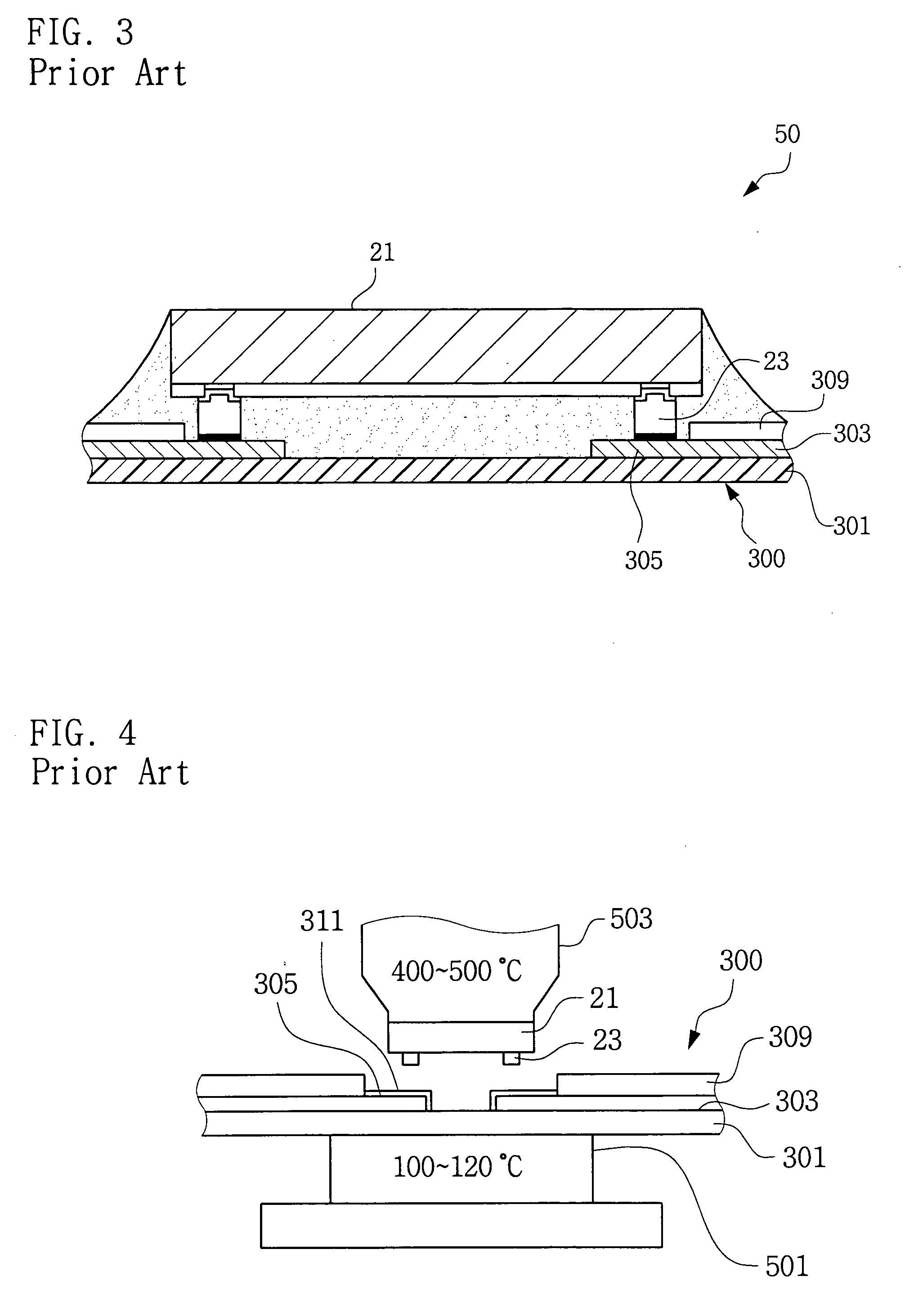
However, a serious shrinkage phenomenon may occur in the conventional film circuit substrate during the chip mounting process.
Such shrinkage of the insulating film due to temperature change may causes misalignment between the semiconductor chip and the film circuit substrate, a loose connection of the gold bump, and damage to the leads.
Consequently, this lowers the quality of the chip mounting and electrical connection, and thereby results in a low-quality sem

Method used


Image

  • Film circuit substrate having Sn-In alloy layer
  • Film circuit substrate having Sn-In alloy layer
  • Film circuit substrate having Sn-In alloy layer

Examples


Example

[0031] Hereinafter, film circuit substrates according to exemplary embodiments of the present invention will now be described in detail with reference to the accompanying drawings. It should be noted that in the following explanation only matters relevant to the understanding of the present invention are explained to avoid obscuring the gist of the present invention. In the same manner, in the accompanying drawings some elements are exaggerated, omitted, or just outlined in brief, and may be not drawn to scale.

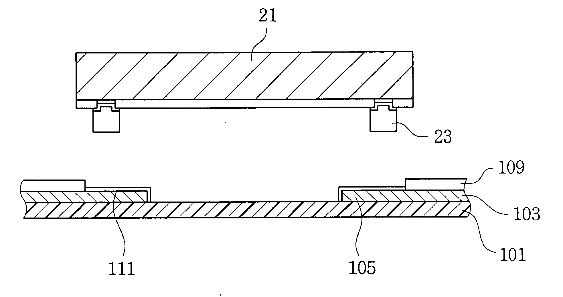
[0032]FIGS. 6 and 7 are partial sectional views showing a film circuit substrate according to the present invention. FIG. 8 is an enlarged sectional view showing a circuit pattern of the film circuit substrate according to the present invention. FIG. 9 is a composition ratio (horizontal axis) v. temperature (vertical axis) graph showing melting points of the tin-indium alloy that is utilized for the film circuit substrate according to the present invention. FIG. 10 is a parti...


PUM


Abstract

In one embodiment, a film circuit substrate comprises an insulating film made of polyimide resin; a conductive circuit pattern formed on the insulating film, the circuit pattern including an inner lead to be connected with a conductive bump of a semiconductor chip through a bump bonding process; and a tin-indium alloy layer formed on the inner lead to produce an inter-metallic compound layer of AuxSn composition during the bump bonding process.

Description

CROSS REFERENCE TO RELATED APPLICATIONS [0001] This U.S. non-provisional application claims benefit of priority under 35 U.S.C. §119 of Korean Patent Application No. 2004-84517, filed on Oct. 21, 2004, the entire contents of which are incorporated herein by reference. BACKGROUND OF THE INVENTION [0002] 1. Field of the Invention [0003] The present invention relates to a film circuit substrate, more specifically, to a film circuit substrate that enables connection of inner leads with gold bumps of a semiconductor chip through inner-lead bonding at a lower temperature. [0004] 2. Description of the Related Art [0005] Corresponding to rapid technical advances in semiconductor devices toward higher integration and thinness, there have been great advances in assembly technologies for manufacturing semiconductor packages. As portable electronic equipment becomes smaller in size and lighter in weight, its market demand has rapidly expanded worldwide. In liquid crystal display (LCD) panel mar...

Claims


Application Information

Patent Timeline
IPC IPC(8): H01L23/58
CPCH01L24/81H01L2224/13144H01L2224/16H01L2224/75H01L2224/75251H01L2224/75252H01L2224/75301H01L2924/01029H01L2924/01049H01L2924/01078H01L2924/01079H01L2924/01082H01L2924/14H05K1/189H05K3/244H05K3/3436H05K3/3463H05K3/3473H05K2201/10674H01L2924/00014H01L2224/81825H01L2224/8181H01L2924/01006H01L2924/01023H01L2924/01033H01L2924/0105H01L2924/014H01L2224/136H01L2224/05001H01L2224/05026H01L2224/05572H01L2924/351H01L2924/00H01L2224/05599H01L2224/05099H01L23/12H01L23/48H01L23/498H01L21/60
Inventor KANG, UN-BYOUNGLEE, CHUNG-SUNKANG, SA-YOONKWON, YONG-HWAN
Owner SAMSUNG ELECTRONICS CO LTD
Why Eureka
Try Eureka