Diffusion barrier for damascene structures

a damascus and diffusion barrier technology, applied in the field of simiconductor structure, can solve the problems of increasing reducing the size of cmos devices, and facing significant challenges

Inactive Publication Date: 2006-05-11
TAIWAN SEMICON MFG CO LTD
View PDF25 Cites 26 Cited by
  • Summary
  • Abstract
  • Description
  • Claims
  • Application Information

AI Technical Summary

Benefits of technology

[0006] These and other problems are generally solved or circumvented, and technical advantages are generally achieved, by preferred embodiments of the present invention which provides a semiconductor structure with a barrier layer in a damascene opening.

Problems solved by technology

Significant challenges, however, are faced as the sizes of CMOS devices continue to decrease.
One such challenge is the fabrication of interconnect structures.
The sidewall of the openings may be damaged during an etching and / or ashing process while forming the openings.
The damaged sidewalls of the openings in the porous low-K dielectric layer may become more porous and rougher.
As a result, a barrier layer formed over the sidewalls of the openings may be non-uniform, thereby allowing conductive material to diffuse into the porous low-K materials.
In these situations, the non-uniform barrier layer may not provide an adequate diffusion barrier.
This diffusion may result in failures and other reliability problems, particularly as design sizes decrease.

Method used


Image

  • Diffusion barrier for damascene structures
  • Diffusion barrier for damascene structures
  • Diffusion barrier for damascene structures

Examples


Embodiment Construction

[0017] The making and using of the presently preferred embodiments are discussed in detail below. It should be appreciated, however, that the present invention provides many applicable inventive concepts that can be embodied in a wide variety of specific contexts. The specific embodiments discussed herein are merely illustrative of specific ways to make and use the invention, and do not limit the scope of the invention.

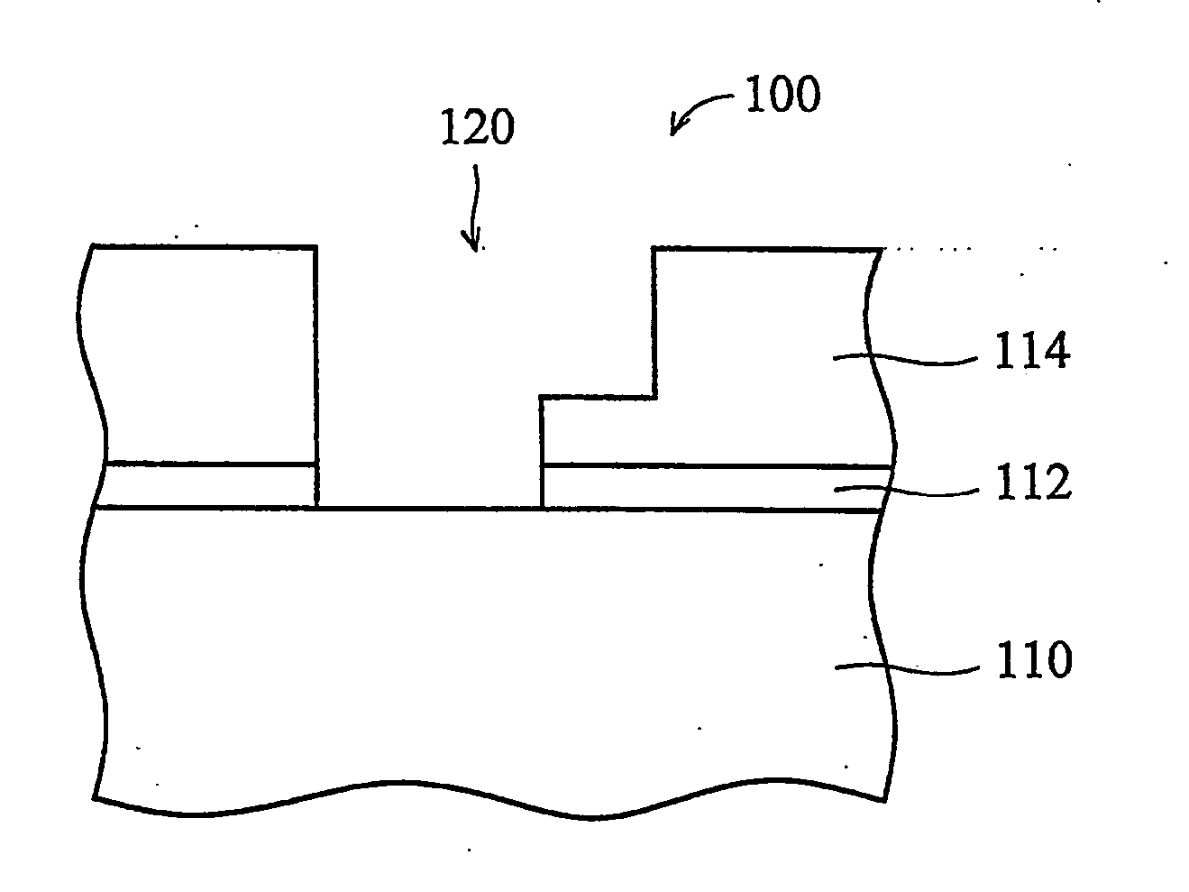
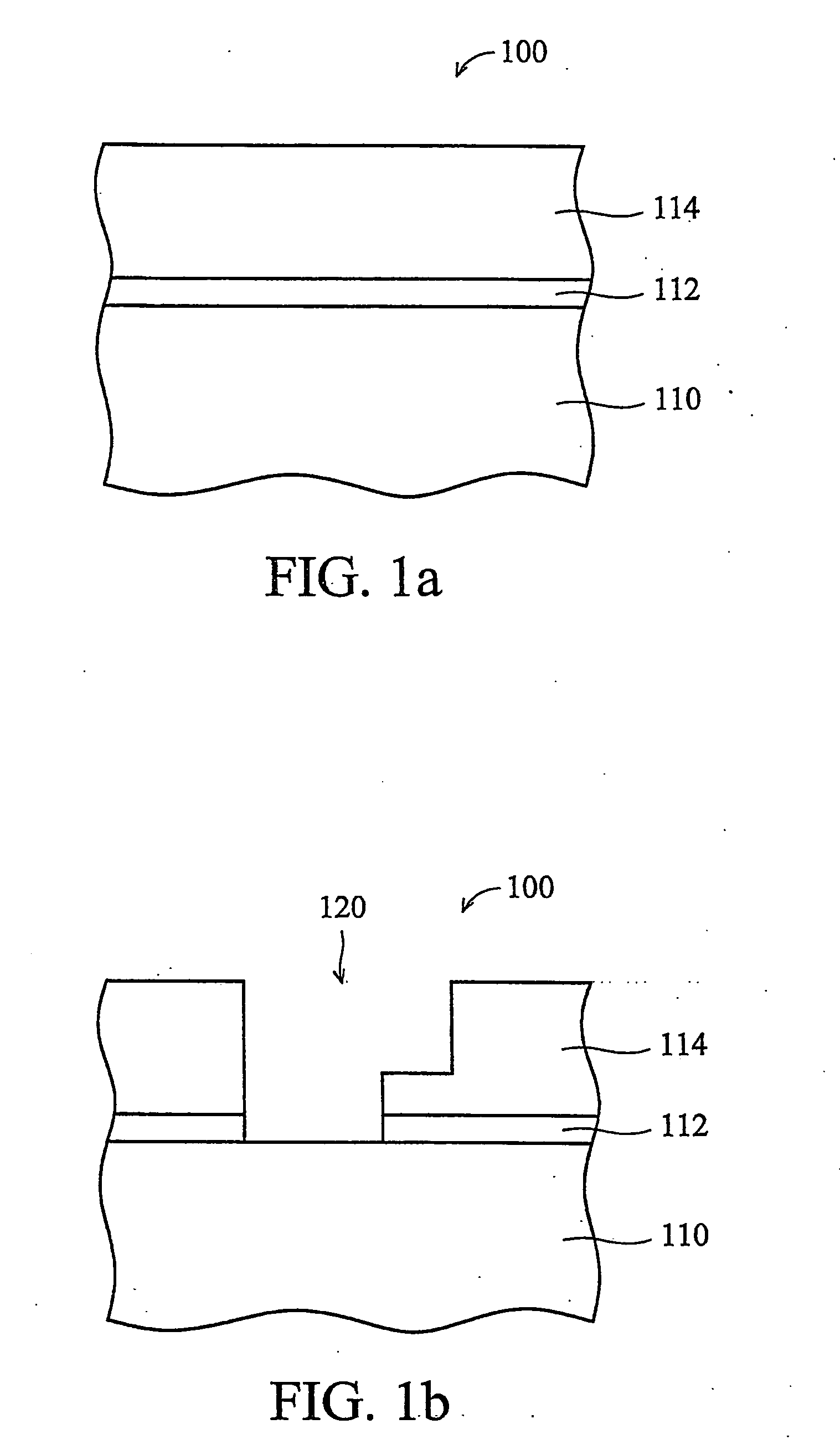
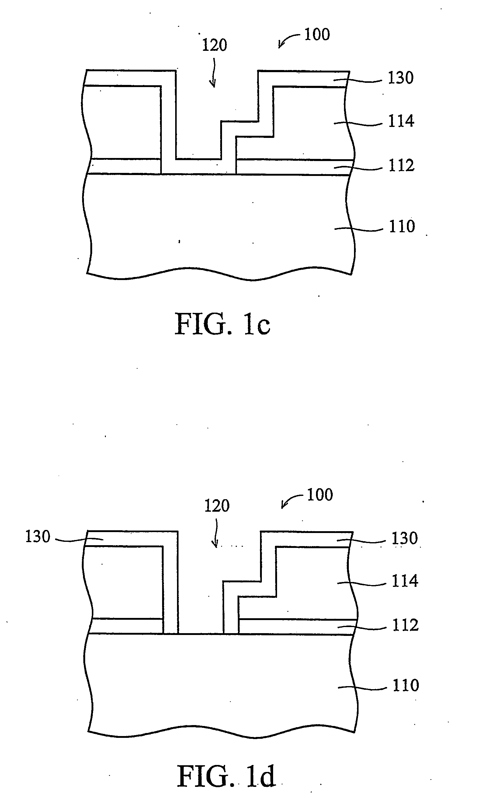
[0018] Referring now to FIG. 1a, a substrate 100 is provided having a conductive layer 110, an etch stop layer 112, and an IMD layer 114. Although it is not shown, the substrate 100 may include circuitry and other structures. For example, the substrate 100 may have formed thereon transistors, capacitors, resistors, interconnects and the like. In an embodiment, the conductive layer 110 is a metal layer that is in contact with electrical devices or another metal layer.

[0019] The conductive layer 110 may be formed of any conductive material, but an embodiment of the pr...


PUM

PropertyMeasurementUnit
dielectric constantaaaaaaaaaa
temperatureaaaaaaaaaa

Abstract

A semiconductor structure having a via formed in a dielectric layer is provided. The exposed pores of the dielectric material along the sidewalls of the via are partially or completely sealed. Thereafter, one or more barrier layers may be formed and the via may be filled with a conductive material. The barrier layers formed over the sealing layer exhibits a more continuous barrier layer. The pores may be partially or completely sealed by performing, for example, a plasma process in an argon environment.

Description

TECHNICAL FIELD [0001] The present invention relates generally to semiconductors and, more particularly, to a semiconductor structure with a barrier layer in a damascene opening and a method for forming such a semiconductor structure in an integrated circuit. BACKGROUND [0002] Complementary metal-oxide-semiconductor (CMOS) technology is the dominant semiconductor technology used for the manufacture of ultra-large scale integrated (ULSI) circuits today. Size reduction of the semiconductor structures has provided significant improvement in the speed, performance, circuit density, and cost per unit function of semiconductor chips over the past few decades. Significant challenges, however, are faced as the sizes of CMOS devices continue to decrease. [0003] One such challenge is the fabrication of interconnect structures. CMOS devices typically include semiconductor structures, such as transistors, capacitors, resistors, and the like, formed on a substrate. One or more conductive layers ...

Claims


Application Information

Patent Timeline
Patent Type & Authority Applications(United States)
IPC IPC(8): H01L21/4763
CPCH01L21/76814H01L21/76826H01L21/76831
Inventor LIN, JING-CHENGSHUE, SHAU-LIN
Owner TAIWAN SEMICON MFG CO LTD
Why Eureka
Try Eureka