Method for producing group iii nitride semiconductor

a nitride semiconductor and semiconductor technology, applied in the direction of crystal growth process, polycrystalline material growth, coating, etc., can solve the problems of unfavorable production efficiency, increased occurrence of ungrown region or abnormal grain growth region, and more remarkably worsened yield ratio, so as to improve yield ratio, uniform thickness, and crystallinity of group iii nitride semiconductor.

Active Publication Date: 2018-03-08
TOYODA GOSEI CO LTD
View PDF6 Cites 1 Cited by
  • Summary
  • Abstract
  • Description
  • Claims
  • Application Information

AI Technical Summary

Benefits of technology

[0014]The mask is preferably formed through ALD. The mask can be formed so as to be dense and have a uniform thickness, thereby preventing the disappearance of the mask due to melting back at an initial growth stage of Group III nitride semiconductor crystal through a flux method. The mask may be made of Al2O3, TiO2, or ZrO2.
[0015]The diameter of the seed substrate is preferably two inches or more. The larger the diameter of the seed substrate, the higher the occurrence of ungrown region or abnormal grain growth region. When the diameter exceeds two inches, this tendency is remarkable. In the present invention, even if the seed substr

Problems solved by technology

However, when GaN is grown on the seed substrate, ungrown region or abnormal grain growth region may occur.
Moreover, abnormal grain growth region is a region where crystal grains are extremely large compared to other regions.
There was a problem that particularly when the seed substrate having seed crystal regions scattered in a dotted pattern is employed, the occurrence of

Method used


Image

  • Method for producing group iii nitride semiconductor
  • Method for producing group iii nitride semiconductor
  • Method for producing group iii nitride semiconductor

Examples


embodiment 1

[0075]The method for producing a GaN crystal according to Embodiment 1 will be described with reference to FIGS. 5 and 6.

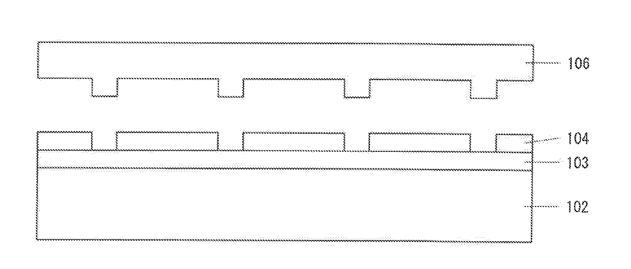
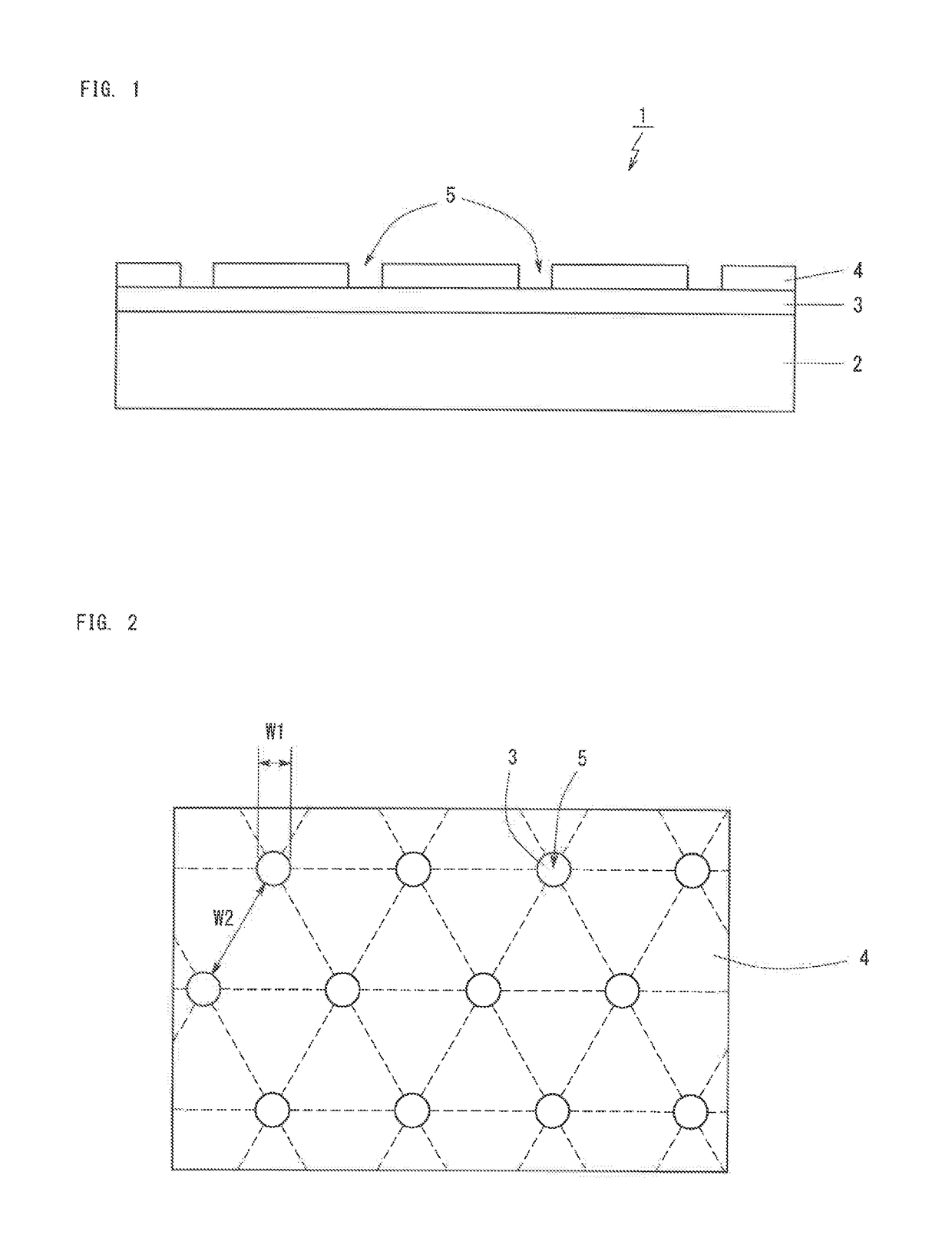
[0076]Firstly, a seed substrate 1 for growing a GaN crystal was prepared as follows. A ground substrate 102 made of sapphire having a diameter of two inches and a thickness of 1 mm was prepared. On the ground substrate 102, an AIN buffer layer (not illustrated) and a GaN layer 103 were sequentially formed through MOCVD (FIG. 5A). The thickness of the GaN layer 103 was 5 μm. In MOCVD, ammonia gas (NH3) was employed as a nitrogen source. Trimethylgallium (Ga(CH3)3: TMG) was employed as a Ga source. Trimethylaluminum (Al(CH3)3: TMA) was employed as an Al source. Hydrogen (H2) was employed as a carrier gas.

[0077]Next, through ALD, on the GaN layer 103, a mask 104 made of Al2O3 was formed (FIG. 5B). The thickness of the mask 104 was 0.1 μm.

[0078]Subsequently, the mask 104 was patterned through photolithography or wet etching to form windows 105 in a triangular lattice ...

embodiment 2

[0086]Instead of the seed substrate 1 according to Embodiment 1, a free-standing seed substrate made of GaN was employed as a substrate. A GaN crystal was grown on the seed substrate same as in Embodiment 1. However, the mask 104 was not formed on the seed substrate. When the grown GaN crystal was observed visually and with an optical microscope, ungrown region or abnormal grain growth region, and inclusion were hardly found. The GaN crystal had little irregularities on the surface thereof and had a high surface flatness. The thickness of the GaN crystal was the same as in Embodiment 1, and the GaN crystal could be efficiently grown.

embodiment 3

[0087]Instead of the seed substrate 1 according to Embodiment 1, the seed substrate 1 having no mask 4 was employed as a seed substrate. That is, a template substrate with the entire surface of the GaN layer 103 exposed was employed. A GaN crystal was grown on the seed substrate in the same way as in Embodiment 1. When the grown GaN crystal was observed visually and with an optical microscope, same as in Embodiment 2, ungrown region or abnormal grain growth region, and inclusion were hardly found. The GaN crystal had little irregularities on the surface thereof and had a high surface flatness. The thickness of the GaN crystal was the same as in Embodiment 1, and the GaN crystal could be efficiently grown.


PUM

PropertyMeasurementUnit
Diameteraaaaaaaaaa
Concentrationaaaaaaaaaa
Semiconductor propertiesaaaaaaaaaa

Abstract

To reduce ungrown region or abnormal grain growth region in growing a Group III nitride semiconductor through a flux method. A seed substrate has a structure in which a Group III nitride semiconductor layer is formed on a ground substrate as a base, and a mask is formed on the Group III nitride semiconductor layer. The mask has a plurality of dotted windows in an equilateral triangular lattice pattern. A Group III nitride semiconductor is grown through flux method on the seed substrate. Carbon is placed on a lid of a crucible holing the seed substrate and a molten mixture so that carbon is not contact with the molten mixture at the start of crystal growth. Thereby, carbon is gradually added to the molten mixture as time passes. Thus, ungrown region or abnormal grain growth region is reduced in the Group III nitride semiconductor crystal grown on the seed substrate.

Description

BACKGROUND OF THE INVENTIONField of the Invention[0001]The present invention relates to a method for producing a Group III nitride semiconductor through a flux method.Background Art[0002]As a method for growing a Group III nitride semiconductor crystal, a flux method is known, in which nitrogen is dissolved in a molten mixture of alkali metal and Group III element such as Ga, and a Group III nitride semiconductor is epitaxially grown in liquid phase. A flux method in which Na (sodium) is generally used as alkali metal, is referred to as the Na flux method.[0003]In the Na flux method, a seed substrate (template substrate) having a GaN layer grown through MOCVD or a similar technique on a ground substrate made of sapphire or a similar material is employed, and GaN is grown on the seed substrate. When such a seed substrate is employed, a part of the GaN layer is removed to form a periodic dotted pattern, or the surface of the GaN layer is covered with a mask, and windows are formed in ...

Claims


Application Information

Patent Timeline
IPC IPC(8): C30B19/02H01L21/02H01L21/78C30B29/40C30B19/12C23C16/34C23C16/56C23C16/455
CPCC30B19/02H01L21/0242H01L21/02458H01L21/0254H01L21/02642C23C16/45525C30B29/406C30B19/12C23C16/34C23C16/56H01L21/7813C30B29/403H01L21/02389H01L21/02625H01L21/02628H01L21/02647
Inventor MORIYAMA, MIKIYAMAZAKI, SHIROYAKUSHI, YASUHIDE
Owner TOYODA GOSEI CO LTD
Why Eureka
Try Eureka