System and method for plasma induced modification and improvement of critical dimension uniformity

a critical dimension and uniformity technology, applied in the field of integrated circuits, can solve the problems of increasing reducing the uniformity of post lithographic cd, and reducing the number of integrated circuits, so as to improve device performance, functionality and reliability, and reduce post lithographic cd non-uniformity ler.

Active Publication Date: 2006-05-11
GLOBALFOUNDRIES US INC
View PDF11 Cites 10 Cited by
  • Summary
  • Abstract
  • Description
  • Claims
  • Application Information

AI Technical Summary

Benefits of technology

[0017] Advantageously, the DFC plasma etch process adapted for achieving a significant neutral to ion flux ratio is implemented for 90 nm and beyond BEOL, FEOL and MOL technologies (193 nm and future lithography) in which advanced plasma processing is utilized to reduc

Problems solved by technology

Efficient routing of these signals across the device can become more difficult as the complexity and number of integrated circuits are increased.
One of the many challenges associated with the fabrication of the thinwires for 90 nm and beyond CMOS BEOL technologies is the reliable printing of ground rule features (≦140 nm) using 193 nm lithography.
Such post lithographic image roughness or LER is readily transferred during via or trench creation (plasma etch processing); rendering liner and seed conformality difficult.
However, since these change

Method used


Image

  • System and method for plasma induced modification and improvement of critical dimension uniformity
  • System and method for plasma induced modification and improvement of critical dimension uniformity
  • System and method for plasma induced modification and improvement of critical dimension uniformity

Examples


examples

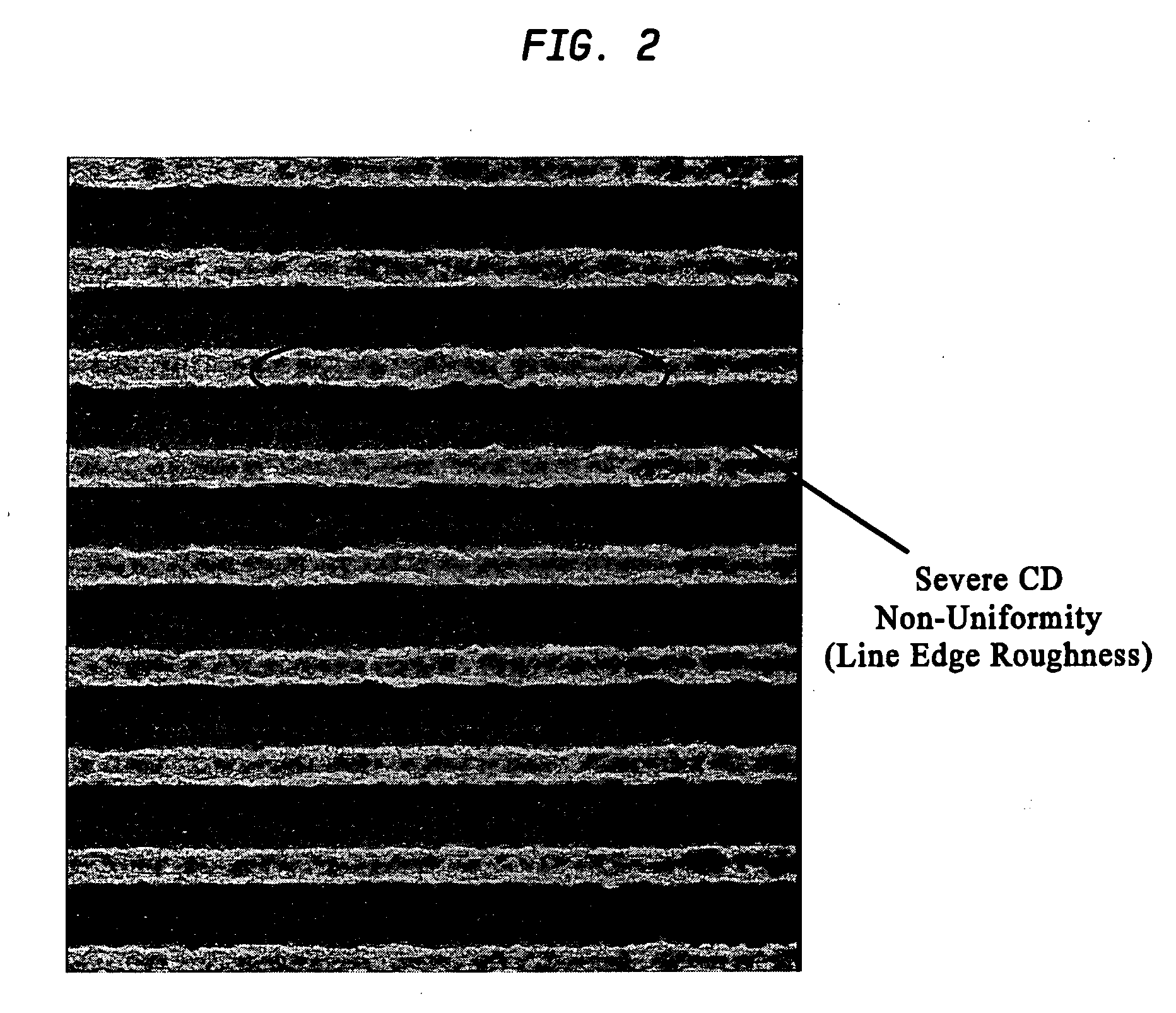
[0028] Three etching conditions (normalized for etch rate differences) are highlighted in FIG. 5 that depicts a table showing percentage improvement in LER for various applied ARC etch chemistries that span the full process parameter space. Each of these three conditions were employed to etch the 200 nm thick ARC layer (shown in FIG. 4) to span the full process parameter space, namely: from “Negligible” (High Etch Rate, High Degree of Etch Anisotropy, and Low Degree of Etch Isotropy) to “Significant” Neutral to Ion Flux Ratio (Low Etch Rate, Low Degree of Etch Anisotropy, and High Degree of Etch Isotropy). The LER associated with each sample was subsequently measured post etch processing and the consequent change in LER (post Lithographic Processing LER—post Etch Processing LER) as a percentage was then determined.

[0029] The data obtained is summarized in Table I (FIG. 5) for each of the three employed etching conditions. It is relevant to note that the “Significant” neutral to ion...


PUM


Abstract

Novel interconnect structures possessing a OSG or polymeric-based (90 nm and beyond BEOL technologies) in which advanced plasma processing is utilized to reduce post lithographic CD non-uniformity (“line edge roughness”) in semiconductor devices. The novel interconnect structure has enhanced liner and seed conformality and is therefore capable of delivering improved device performance, functionality and reliability.

Description

BACKGROUND OF THE INVENTION [0001] 1. Field of the Invention [0002] The present invention generally relates to integrated circuits (ICs), and more particularly to interconnect structures, including multilevel interconnect structures, in which an advanced plasma process is utilized to enable a reduction of critical dimension non-uniformity post lithographic processing; thus improving liner and Cu seed conformality for desired device / interconnect performance, reliability, and functionality. [0003] 2. Description of the Prior Art [0004] Generally, semiconductor devices include a plurality of circuits which form an integrated circuit including chips (e.g., chip back end of line, or “BEOL”), thin film packages and printed circuit boards. Integrated circuits can be useful for computers and electronic equipment and can contain millions of transistors and other circuit elements that are fabricated on a single silicon crystal substrate. For the device to be functional, a complex network of s...

Claims


Application Information

Patent Timeline
IPC IPC(8): H01L21/461H01L47/00H01L21/302
CPCG03F7/40G03F7/405H01L21/0276H01L21/31138H01L21/31144
Inventor DALTON, TIMOTHY J.DELLA GUARDIA, RONALD A.FULLER, NICHOLAS C.
Owner GLOBALFOUNDRIES US INC
Why Eureka
Try Eureka