Semiconductor signal processing device

a signal processing and semiconductor technology, applied in the direction of instruments, computation using denominational number representation, and architecture with multiple processing units, can solve the problems of insufficient dsp, insufficient address area available for data reading and writing by each logic module accessing the multi-port data memory, and large amount of data to be processed

Inactive Publication Date: 2006-05-11
RENESAS TECH CORP
View PDF31 Cites 36 Cited by
  • Summary
  • Abstract
  • Description
  • Claims
  • Application Information

AI Technical Summary

Benefits of technology

[0024] Further, by a configuration in which the same data word is stored in each entry and arithmetic / logic operation is performed in corresponding processing circuits in a bit-serial manner, arithmetic / logic operation can be performed even when word configuration (bit width) of the data is changed, without necessitating significant change in hardware.

Problems solved by technology

Therefore, an address area available for data reading and writing by each logic module accessing the multi-port data memories is limited.
When the amount of data to be processed is very large, even a dedicated DSP is insufficient to attain dramatic improvement in performance.
Therefore, although each process can be done at high speed in an arrangement in which the sum-of-products operation is performed using a register file as described in Reference 1, when the amount of data increases, the time of processing increases in proportion thereto as the data are processed in series, and therefore, such an arrangement cannot achieve high speed processing for a large amount of data.
When a dedicated DSP is used, the processing performance much depends on an operating frequency, and therefore, if high speed processing were given priority, power consumption would considerably be increased.
When the arrangement is to be diverted to other application, the bit width, configuration of processing circuit and the others must be re-designed, and hence, it lacks flexibility for a plurality of different applications including arithmetic / logic operations.
This means that data transfer takes time, the machine cycle cannot be made shorter and hence, high speed processing is hindered.
Assume that data of one pixel consists of 8 bits and one line has 512 pixels, the number of memory cells of one row of memory cells will be 8×512=4 k bits, a row selecting line (word line) connecting to one row of memory cells has an increased load, and it becomes difficult to select at high speed the memory cells for transferring data between the operational processing portion and the memory cells, hindering high speed processing.
Therefore, because of line capacitance and the like, high-speed data transfer is difficult, and even when pipeline processing is performed, the machine cycle of the pipeline cannot be made shorter.

Method used


Image

  • Semiconductor signal processing device
  • Semiconductor signal processing device
  • Semiconductor signal processing device

Examples


first embodiment

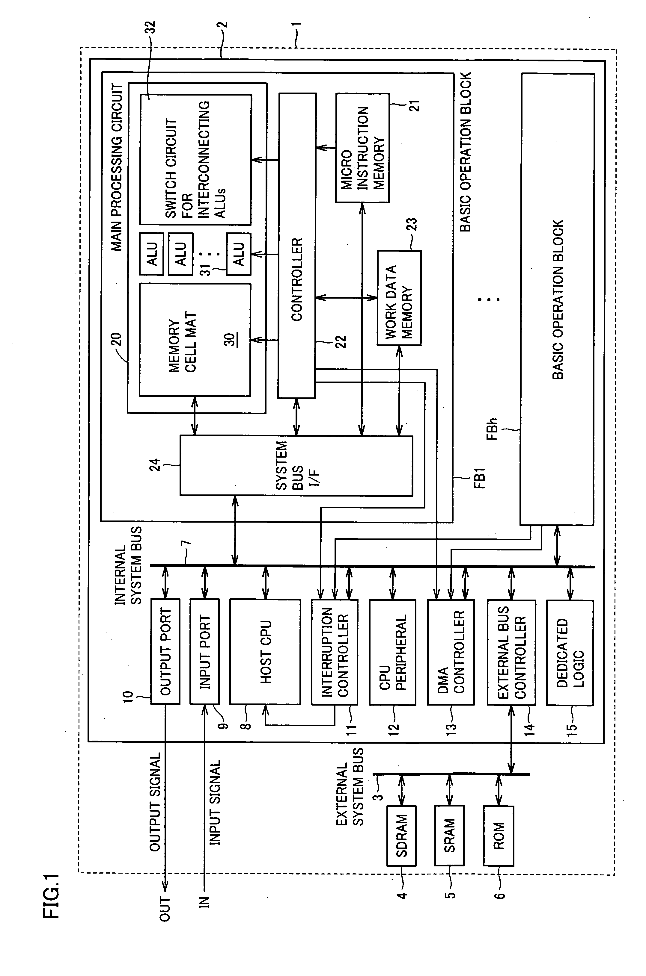
[0057]FIG. 1 schematically shows an overall configuration of the processing system in which the semiconductor signal processing device according to the present invention is used. Referring to FIG. 1, the signal processing system 1 includes a system LSI 2 implementing arithmetic / logic functions for executing various processes, and an external memory connected to system LSI 2 through an external system bus 3. The external memory includes a large capacity memory 4, a high speed memory 5, and a read only memory (ROM) 6 for storing fixed information such as boot instructions. Large capacity memory 4 is formed, for example, of a clock-synchronous type dynamic random access memory (SDRAM), and high speed memory 5 is formed, for example, of a static random access memory (SRAM).

[0058] The specific configuration of the shown system LSI is disclosed in a co-pending U.S. patent Application, U.S. Ser. No. 11 / 148,369, commonly assigned to the assignee of the present application. The contents of ...

second embodiment

[0130]FIG. 10 schematically shows a configuration of the basic operation block FBi according to the second embodiment of the present invention. In basic operation block FBi shown in FIG. 10, the following configuration of controller 22 is different from that of controller 22 according to the first embodiment shown in FIG. 6 described above. Specifically, controller 22 includes a start address register 70 for storing a start address of the loop when a loop instruction is executed, and an end address register 72 for storing a loop end address. Values stored in start address register 70 and end address register 72 are applied to a PC value calculating unit 42. Except for this point, the configuration of controller 22 shown in FIG. 10 is the same as that of controller 22 shown in FIG. 6. Therefore, corresponding portions are denoted by the same reference characters and detailed description will not be repeated.

[0131] In the second embodiment, a loop instruction LOOP is additionally pre...

third embodiment

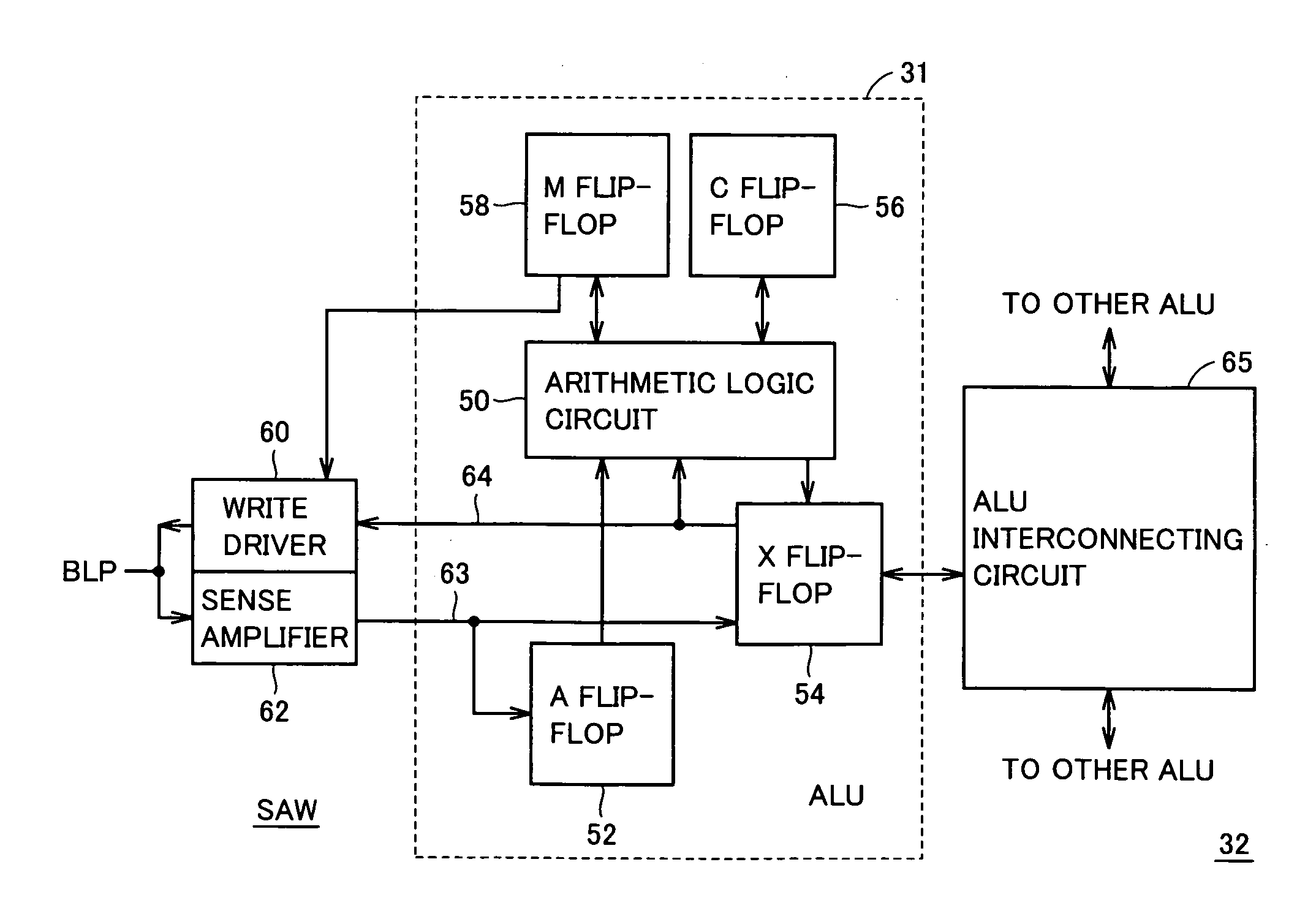
[0148]FIG. 13 schematically shows a configuration of the basic operation block FBi according to the third embodiment of the present invention. Referring to FIG. 13, main processing circuit 20 includes two memory mats 30A and 30B. For memory cell mats 30A and 30B, read / write circuits 38A and 38B are provided, respectively. Memory cell mats 30A and 30B have the same configuration, and are each divided into a plurality of entries ERY. In read / write circuits 38A and 38B, for each entry ERY, a sense amplifier and write driver SAW is provided.

[0149] The memory cell mats 30A and 30B are coupled to the corresponding ALUs 31 included in the arithmetic logic unit 35 through mutually separate bit line pairs. Therefore, memory cell mats 30A and 30B can be accessed individually and separately. Main processing circuit 20 further includes, as in the first and second embodiments described above, switch circuit 32 for interconnecting ALUs, for switching connection path between ALUs 31 in arithmetic...


PUM


Abstract

An instruction for an arithmetic/logic operation to a main processing circuit is stored in the form of a micro program in a micro instruction memory, and the operation of the main processing circuit is controlled in accordance with the micro program, under the control of a controller. In the main processing circuit, a memory mat is divided into entries each storing data of a plurality of bits, and for each entry, a processor (ALU) is arranged. Arithmetic/logic operations are performed entry-parallel and in bit-serial manner between each entry and the associated ALU. In accordance with the micro program control method, a large amount of data can be processed efficiently. Thus, a processing device that efficiently performs an arithmetic/logic operation on a large amount of data at high speed is provided.

Description

CROSS REFERENCE TO RELATED APPLICATION [0001] An invention related to the present application is disclosed in a co-pending application, U.S. Ser. No. 11 / 148,369, commonly assigned to the assignee of the present application.BACKGROUND OF THE INVENTION [0002] 1. Field of the Invention [0003] The present invention relates to a semiconductor signal processing device and, more specifically, to a configuration of a signal processing integrated circuit device employing a semiconductor memory performing an arithmetic / logic operation on a large amount of data at high speed. [0004] 2. Description of the Background Art [0005] Recently, along with wide spread use of portable terminal equipments, digital signal processing allowing high speed processing of a large amount of data including voice or audio and image data comes to have higher importance. For such digital signal processing, generally, a DSP (Digital Signal Processor) is used as a dedicated semiconductor device. Digital signal processi...

Claims


Application Information

Patent Timeline
Patent Type & Authority Applications(United States)
IPC IPC(8): G06F15/00
CPCG06F9/3879G06F9/3897G06F15/8015
Inventor HIGASHIDA, MOTOKI
Owner RENESAS TECH CORP
Why Eureka
Try Eureka