Antifuse structure having an integrated heating element

a technology of heating element and antifuse, which is applied in the direction of semiconductor devices, semiconductor/solid-state device details, instruments, etc., can solve the problems of negative impact on the flow of production testing and repair of new chips, current and the required high voltage are close to integrated circuit design constraints, and no component of the antifuse itself is involved in the generation of heat, etc., to achieve the effect of direct heating of the dielectric layer

Inactive Publication Date: 2006-05-18
GLOBALFOUNDRIES INC
View PDF19 Cites 68 Cited by
  • Summary
  • Abstract
  • Description
  • Claims
  • Application Information

AI Technical Summary

Benefits of technology

[0009] The present invention addresses the above-described problems by facilitating direct heating of a dielectric layer of an antifuse. According to the invention, there is provided novel antifuse structures having an integrated heating element and methods of programming thereof. In accordance with one aspect of the invention, a conventional antifuse and a heating element are integrated into a single structure where the heating element facilitates direct heating of a dielectric layer of the antifuse.

Problems solved by technology

Such required high currents impose minimum size constraints on the antifuses and wiring thereto, thereby requiring significant integrated circuit area to implement, while also negatively affecting the flow of production testing and repair of new chips.
The high programming voltage may give rise to concerns for electrostatic discharge protection (ESD) and the reliability of the integrated circuit.
However, such currents and the required high voltage are close to integrated circuit design constraints based on ESD protection and reliability considerations.
This presents a problem in that the voltage / current required to program the antifuse must pass through standard CMOS logic without damaging it.
Such a solution provides indirect heating, however, no component of the antifuse itself is involved in the generation of the heat.
There are several drawbacks to such a solution utilizing indirect heating.
First, additional processing steps are required to place a heat generation source in proximity to the antifuse.
This requires additional process steps, thus increasing complexity and potential for yield loss.
Second, although sufficient heat may be generated, transferring the heat to the antifuse is inefficient because of the indirect nature of the heating that occurs.
This heat transfer path is inefficient and requires a high programming current to travel through heating element 305 to produce sufficient indirect heating of dielectric layer 330.
Also, some amount of delay will occur from a point in time when the external heating element is activated to when the heat energy reaches the antifuse element.
The dielectric material that separates the external heating element and the antifuse element is typically a poor thermal conductor.
Finally, the overall size of the programmable circuit is increased by adding a separate heating element, thus negatively impacting the size of the integrated circuit on which such antifuse structures reside.

Method used


Image

  • Antifuse structure having an integrated heating element
  • Antifuse structure having an integrated heating element
  • Antifuse structure having an integrated heating element

Examples


first embodiment

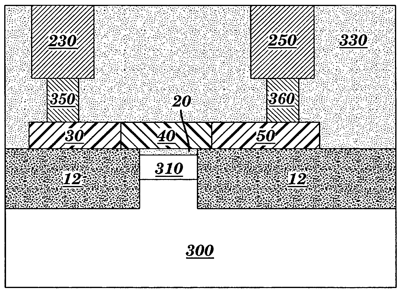
[0033]FIG. 2a illustrates a partial top-down view of an antifuse structure according to the present invention. Programmable circuit 10 includes an isolation layer 12 formed on a semiconductor substrate (not shown) and an antifuse structure formed by a lower conductor (not shown), upper conductor 40, and the portion of dielectric layer 20 formed between the lower and upper conductors. Anode 30 and cathode 50 are formed adjacent an insulating layer (not shown) and formed on isolation layer 12. Anode 30 and cathode 50 source / sink current through the upper conductor 40. Upper conductor 40 is also formed adjacent the insulating layer and formed partially on isolation layer 12 and partially on dielectric layer 20. In one example, upper conductor 40 has a width of approximately 60 nm to 120 nm and a length of approximately 300 nm to 1200 nm. Upper conductor 40 can be formed from any suitable conductive material such as doped and undoped polysilicon, doped and undoped silicided polysilicon,...

second embodiment

[0048]FIG. 4a illustrates a partial top-down view of an antifuse structure according to the present invention. Programmable circuit 500 includes an isolation layer 512 formed on a semiconductor substrate (not shown) and an antifuse structure formed by a lower conductor (not shown), upper conductor 530, and the portion of dielectric layer 520 formed between the lower and upper conductors. Upper conductor 530 is formed adjacent an insulating layer (not shown) and formed partially on isolation layer 512 and partially on dielectric layer 520. Upper conductor 530 can be formed from any suitable conductive material such as doped and undoped polysilicon, doped and undoped silicided polysilicon, doped and undoped monocrystalline silicon, titanium nitride, tantalum nitride, metals including aluminum, copper and alloys thereof, and refractory metals including tungsten, titanium, tantalum and alloys thereof. Dielectric layer 520 is formed on the lower conductor and can be formed from any suita...

third embodiment

[0056]FIG. 5a illustrates a partial top-down view of an antifuse structure according to the present invention. Programmable circuit 800 includes an isolation layer 812 formed on a semiconductor substrate (not shown) and an antifuse structure formed by a lower conductor (not shown), upper conductor 840, and the portion of dielectric layer 820 formed between the lower and upper conductors. Anode 830 and cathode 850 are formed adjacent an insulating layer (not shown) and formed on isolation layer 812. Anode 830 and cathode 850 source / sink current through upper conductor 840. Upper conductor 840 is also formed adjacent the insulating layer and formed partially on isolation layer 812 and partially on dielectric layer 820. Upper conductor 840 can be formed from any suitable conductive material such as doped and undoped polysilicon, doped and undoped silicided polysilicon, doped and undoped monocrystalline silicon, titanium nitride, tantalum nitride, metals including aluminum, copper and a...


PUM


Abstract

The present invention provides antifuse structures having an integrated heating element and methods of programming the same, the antifuse structures comprising first and second conductors and a dielectric layer formed between the conductors, where one or both of the conductors functions as both a conventional antifuse conductor and as a heating element for directly heating the antifuse dielectric layer during programming.

Description

BACKGROUND OF THE INVENTION [0001] The present invention relates to semiconductor structures, and particularly, to antifuse structures having an integrated heating element and methods of programming thereof. [0002] Electrically operable fuses are utilized within the field of integrated circuit devices and processes for a number of purposes, including programming alterable circuit connections, or replacing defective circuit elements with redundant circuit elements. One type of electrically operable fuse, a so-called “antifuse”, is a device having two conductors and an intervening dielectric layer, where the dielectric layer is subject to breakdown upon application of sufficient voltage and current to the conductors. The resistance across the dielectric layer of the antifuse encodes the “on” or “off” state of the antifuse. [0003] A typical (pre-breakdown) “off” resistance for antifuses having a dielectric layer of silicon nitride (SiN), “gate oxide”, i.e. silicon dioxide (SiO2) formed...

Claims


Application Information

Patent Timeline
Patent Type & Authority Applications(United States)
IPC IPC(8): H01L29/00
CPCH01L23/5252H01L2924/3011H01L2924/0002Y10S257/928H01L2924/00G11C17/165G11C2229/763H10B20/20
Inventor PARK, BYEONGIUIYER, SUBRAMANIAN S.KOTHANDARAMAN, CHANDRASEKHERAN
Owner GLOBALFOUNDRIES INC
Why Eureka
Try Eureka