Semiconductor device and method of manufacturing the same

a semiconductor and semiconductor technology, applied in the field of semiconductor devices, can solve the problems of unsuitable large-capacity memory use, high access speed of srams, low access speed of drams, etc., and achieve the effect of reducing the non-uniformity of electrical characteristics and reliability deterioration, and reducing the non-uniformity of characteristics between elements due to a large crystal grain siz

Active Publication Date: 2006-05-18
RENESAS ELECTRONICS CORP
View PDF4 Cites 46 Cited by
  • Summary
  • Abstract
  • Description
  • Claims
  • Application Information

AI Technical Summary

Benefits of technology

[0058] The occurrence of voids due to the growth of the crystal grains of a chalcogenide film in an oblique direction can be suppressed during the manufacturing processes for a semiconductor storage device. This, in turn, makes it possible to suppress the nonuniformity of electrical characteristics and deterioration of reliability that are due to manufacturing process factors relating to phase change memories.
[0059] In-process peeling induced by crystallization can also be prevented. The initial crystallization state and the crystal structure of a set state are close to each other, and characteristics stabilize from the first rewriting operation. The nonuniformity in characteristics between elements due to a large crystal grain size can be reduced.

Problems solved by technology

Although large in capacity, DRAMs are low in access speed.
Conversely, SRAMs are high in access speed, whereas they are unsuitable for use as a large-capacity memory, since they require as many as four to six transistors per cell and are therefore difficult to integrate with high density.
In other words, both are volatile.
Flash memories, however, are nonvolatile, so although they require no electrical energization for memory retention, memories of this type have drawbacks in that the maximum permissible number of their rewriting / erasing operations is limited to about 105 times and in that their rewriting speeds are several orders-of-magnitude lower than other memories.
Additionally, there will be very significant impacts if all types of semiconductor memories become replaceable with a single type of memory.

Method used


Image

  • Semiconductor device and method of manufacturing the same
  • Semiconductor device and method of manufacturing the same
  • Semiconductor device and method of manufacturing the same

Examples


embodiments

[0102] Embodiments of the present invention are described in detail below in accordance with the accompanying drawings.

first embodiment

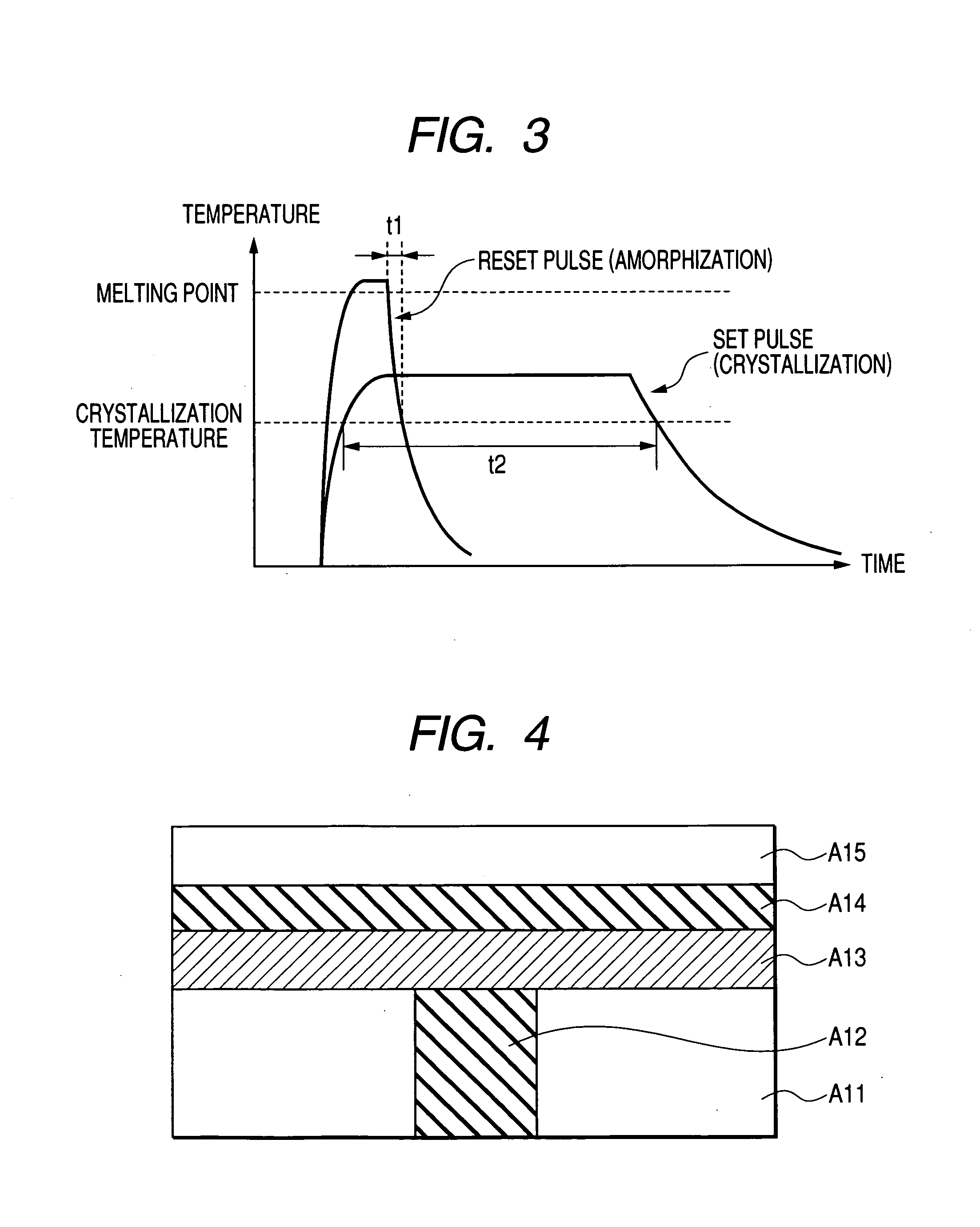
[0103] A first embodiment of the present invention is described below with reference to FIGS. 13 and 14. This embodiment intends to suppress a growth of inclined crystal grains by forming a chalcogenide layer under the conditions that render the chalcogenide layer amorphous and is an example in which first means for forming phase change memory cells in a semiconductor storage device of the present invention is shown in detail.

[0104] As shown in FIG. 13, a semiconductor substrate A101 is prepared for use and an MOS transistor for use as a select transistor is produced. To this end, an inter-element isolation oxide film A102 for isolating the MOS transistor is first formed on the surface of the semiconductor substrate A101 by using a well-known selective deposition method or trench isolation method. The present embodiment employs the trench isolation method that allows surface planarization.

[0105] First, an isolation trench is formed in the substrate by using a well-known dry-etchin...

second embodiment

[0125] A second embodiment of the present invention is described below with reference to FIGS. 13 and 14. This embodiment intends to suppress a growth of inclined crystal grains by post-annealing a chalcogenide layer and forming an “fcc” crystal of a columnar structure, and is an example in which the second means for forming phase change memory cells in the above-mentioned semiconductor storage device of the present invention is shown in detail.

[0126] The description of FIG. 13 is omitted since processes up to forming a tungsten plug A112 are the same as in the first embodiment. After the formation of the plug A112, a chalcogenide layer A113 formed of a 100-nm-thick GeSbTe film in an amorphous phase is deposited using a sputtering method.

[0127] The deposition is followed by 200° C. three-minute annealing in an argon (Ar) atmosphere. This annealing process forms GeSbTe into such an “fcc” crystal of a columnar structure as shown in FIG. 11. A temperature of 100° C. or more and up to...


PUM

PropertyMeasurementUnit
temperatureaaaaaaaaaa
thicknessaaaaaaaaaa
temperatureaaaaaaaaaa

Abstract

The annealing process at 400° C. or more required for the wiring process for a phase change memory has posed the problem in that the crystal grains in a chalcogenide material grow in an oblique direction to cause voids in a storage layer. The voids, in turn, cause peeling due to a decrease in adhesion, variations in resistance due to improper contact with a plug, and other undesirable events. After the chalcogenide material has been formed in an amorphous phase, post-annealing is conducted to form a (111)-oriented and columnarly structured face-centered cubic. This is further followed by high-temperature annealing to form a columnar, hexagonal closest-packed crystal. Use of this procedure makes it possible to suppress the growth of inclined crystal grains that causes voids, since crystal grains are formed in a direction perpendicular to the surface of an associated substrate.

Description

CLAIM OF PRIORITY [0001] The present application claims priority from Japanese application JP 2004-330537, filed on Nov. 15, 2004, and Japanese application JP 2005-010199, filed on Jan. 18, 2005, the contents of which are hereby incorporated by reference into this application. BACKGROUND OF THE INVENTION [0002] 1. Field of the Invention [0003] The present invention relates to a technique applied to and effective for a semiconductor device having a phase change memory cell formed using a phase change material such as chalcogenide. [0004] 2. Description of the Related Arts [0005] Mobile devices represented by hand-held phones use a semiconductor memory such as a DRAM, SRAM, or flash memory. Although large in capacity, DRAMs are low in access speed. Conversely, SRAMs are high in access speed, whereas they are unsuitable for use as a large-capacity memory, since they require as many as four to six transistors per cell and are therefore difficult to integrate with high density. [0006] Al...

Claims


Application Information

Patent Timeline
Patent Type & Authority Applications(United States)
IPC IPC(8): H01L21/20
CPCC23C14/0623C23C14/541C23C14/5806H01L27/2436H01L27/2463H01L45/06H01L45/144H01L45/1625H01L45/1641H10B63/30H10B63/80H10N70/231H10N70/8828H10N70/026H10N70/041
Inventor MATSUI, YUICHITERAO, MOTOYASUTAKAURA, NORIKATSUMORIKAWA, TAKAHIROYAMAMOTO, NAOKI
Owner RENESAS ELECTRONICS CORP
Why Eureka
Try Eureka