Method for producing printed wiring board

a technology of printed wiring and printed circuit, which is applied in the direction of printed circuit manufacturing, printed circuit aspects, connection contact member materials, etc., can solve the problems of blistering, affecting the bend performance of the same, and the failure of electronic devices, so as to improve the contact performance and bond strength between the conductor portion and the insulating resin layer, the effect of improving the bond strength and improving the bond strength

Inactive Publication Date: 2006-05-25
SHARP KK
View PDF8 Cites 9 Cited by
  • Summary
  • Abstract
  • Description
  • Claims
  • Application Information

AI Technical Summary

Benefits of technology

[0012] The present invention is carried out in view of the above-described problems, and has an object of providing a method for producing a printed wiring board having superiority in all of the reliability, durability, and product stability by drastically improving the contact performance and the bond strength between an interlayer insulating layer and a conductor layer without reducing the bend performance through active formation and utilization of projecting metal crystals on the surface of a conductor portion.

Problems solved by technology

For example, in a multilayer wiring board, an insufficient bond strength between an interlayer insulating layer and a conductor metal layer can break the wiring board or disconnect the circuits, which can lead to malfunction of an electronic device that has the wiring board mounted thereon, because the layers may separate from one another when a temperature stress or a bend stress is applied to the wiring board.
It is also known, especially with a printed wiring board that has flexibility, such as flexible wiring board and flex-rigid wiring board, that the contact property and the bond performance between a conductor layer and the insulating layers that are placed above and below it not only cause a problem of blisters due to temperature and moisture stresses but also affect the bend performance of the same.
In reality, however, they do not always result in improvement in the contact property and the bond property between the layers.
Since a flexible wiring board is made by bonding polyimide that is difficult to bond and a copper film, there is a reality in which the above mentioned methods may not always be able to secure a sufficient bond strength between the cover lay and the conductor pattern at the portion bended as mentioned above.

Method used


Image

  • Method for producing printed wiring board
  • Method for producing printed wiring board
  • Method for producing printed wiring board

Examples


embodiment 1

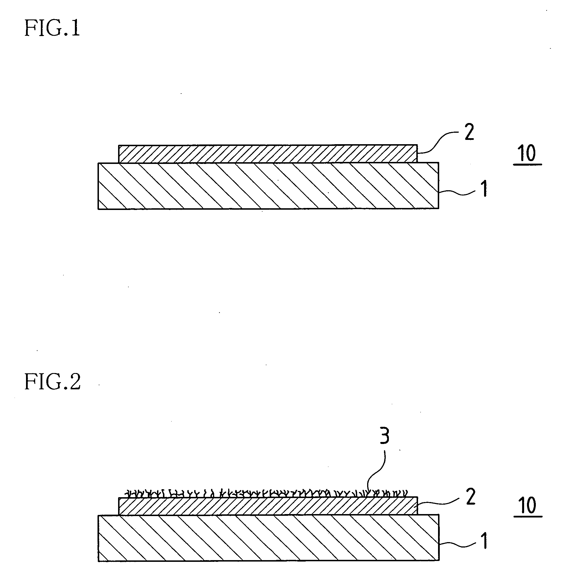
[0045] FIGS. 1 to 3 are schematic cross-sectional views of an enlarged conductor portion of a printed wiring board according to Embodiment 1 of the present invention.

[0046] A printed wiring board 10 is a flexible wiring board that has a conductor pattern formed as a conductor portion 2 (not shown) on one side (the side that becomes an outer side after laminating) of a wiring board substrate 1 that is made of a polyimide or polyester film. The conductor pattern on the wiring board substrate 1 is formed with a copper film. Although it is not shown in FIG. 1, an adhesive layer may be provided between a conductor of the conductor pattern and the wiring board substrate 1. First, an appropriate plating pretreatment is performed on the surface of the conductor of the conductor pattern of the wiring board substrate 1.

[0047] Next, projecting metal crystals are formed on the surface of the above mentioned conductor portion 2 using an electroplating method or a chemical plating method. In th...

embodiment 2

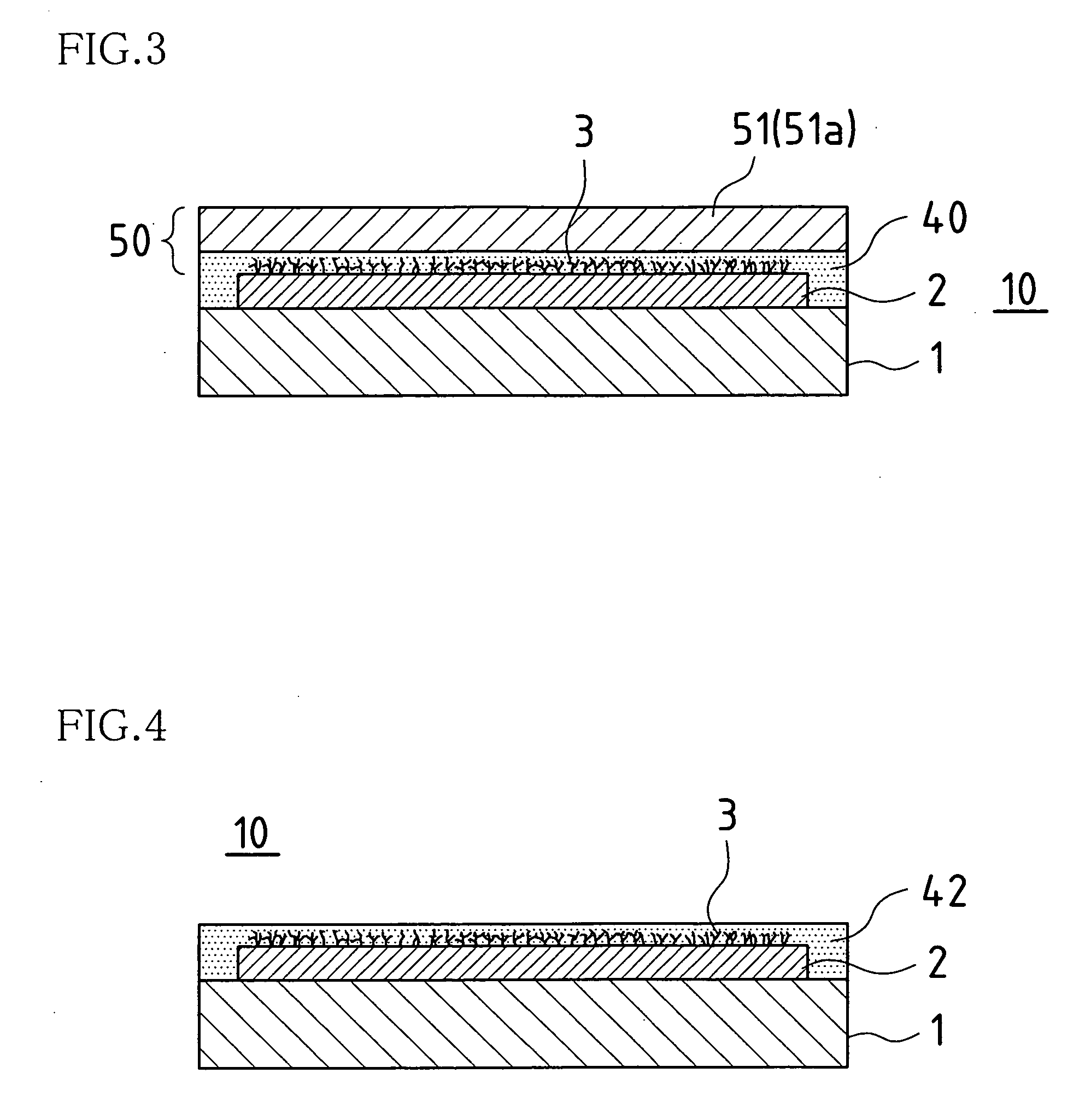
[0055] Hereafter, Embodiment 2 of the present invention will be described. FIGS. 4 and 5 are schematic cross-sectional views that show Embodiment 2 according to the present invention. In each explanation of a method for producing a printed wiring board according to Embodiments 2 to 6, the detailed explanations are omitted by using the same numeric references for the portion that has the same configuration as Embodiment 1.

[0056] As shown in FIG. 4, in Embodiment 2, numerous dendrites 3 are formed on a conductor pattern 2, and, subsequently, an adhesive 42 in a flowing liquid state is applied onto the wiring board substrate 1 and filled into the spaces between the dendrites 3. In this embodiment, a denatured acrylic adhesive is used as the adhesive 42.

[0057] The adhesive 42 may be applied in a method as required by the properties of the adhesive used, such as in a roll coating method, a spray method and a printing method, and is applied and filled so that the spaces between the dend...

embodiment 3

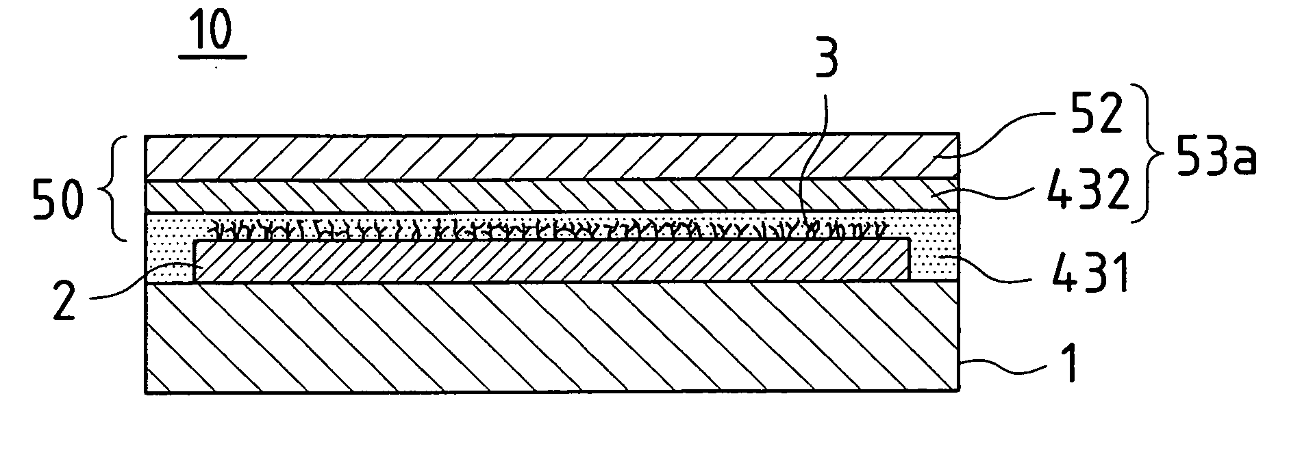
[0060] Hereafter, Embodiment 3 of the present invention will be described. FIGS. 6 and 7 are schematic cross-sectional views that show Embodiment 3 of the present invention. This embodiment may be interpreted as a combination of Embodiments 1 and 2 described above.

[0061]FIG. 6 shows a state in which numerous dendrites 3 have been formed on the surface of a conductor portion 2 and a liquid adhesive 431 has been applied thereon in the same manner as in Embodiments 1 and 2.

[0062] An insulating resin layer 50 is then formed. In the illustrated example, the insulating resin layer 50 is formed by laminate bonding a cover lay material 53a that has an adhesive layer in a semi-cured state formed thereon by applying in advance an adhesive 432 to a polyimide film, polyester film, or the like serving as an insulating resin plate 52.

[0063] Next, as shown in FIG. 7, after the adhesive 431 that has been applied onto a wiring board substrate 1 and filled into the dendrites 3 becomes semi-cured o...


PUM

PropertyMeasurementUnit
pressureaaaaaaaaaa
temperatureaaaaaaaaaa
timeaaaaaaaaaa

Abstract

An insulating resin layer 50 is formed on a surface of a conductor portion 2 by performing a plating pretreatment to the conductor portion 2 that has been formed on a surface of a wiring board substrate 1, and forming numerous dendrites 3 on the surface of the conductor portion 2 using an electroplating or chemical plating method. The insulating resin layer 50 is then formed by stacking an insulating resin plate 50 that has a semi-cured adhesive layer 40 formed thereon in advance on the conductor portion 2 and the dendrites 3, and then applying pressure and raising temperature for laminate bonding.

Description

BACKGROUND OF THE INVENTION [0001] This application claims priority under 35 U.S.C. § 119(a) on Patent Application No. 2004-336145 filed in Japan on Nov. 11, 2004, the entire contents of which are hereby incorporated by reference. [0002] The present invention relates to a method for producing a printed wiring board. [0003] In general, a printed wiring board is produced after undergoing many processes for laminating and bonding a conductor layer and an insulating layer. In these production processes, it is a very important factor to secure the bond strength by improving the contact performance between layers of a printed wiring board. [0004] For example, in a multilayer wiring board, an insufficient bond strength between an interlayer insulating layer and a conductor metal layer can break the wiring board or disconnect the circuits, which can lead to malfunction of an electronic device that has the wiring board mounted thereon, because the layers may separate from one another when a ...

Claims


Application Information

Patent Timeline
Patent Type & Authority Applications(United States)
IPC IPC(8): H05K1/02H05K1/09H05K1/00
CPCH05K1/0393H05K3/243H05K3/281H05K3/384H05K3/386H05K3/4635H05K2201/0195H05K2203/0307H05K2203/0315H05K2203/072H05K2203/0723H05K2203/0759
Inventor UENO, YUKIHIRO
Owner SHARP KK
Why Eureka
Try Eureka