Exposure method and apparatus, exposure mask, and device manufacturing method

Inactive Publication Date: 2006-05-25
CANON KK
View PDF20 Cites 14 Cited by
  • Summary
  • Abstract
  • Description
  • Claims
  • Application Information

AI Technical Summary

Benefits of technology

[0020] In accordance with the present invention, even if the spacing between adjacent openings is close to the wavelength of light or shorter, there is no possibility that near field lights leaking from the adjacent openings of the mask are superposed one upon another. Thus, the present invention can achieve an exposure method and apparatus, an exposure mask and a device man

Problems solved by technology

While the fineness is being improved in the optical lithography, in order to assure microprocessing of 0.1 μm or narrower, there still remain many unsolved problems such as further shortening of laser, development of lenses usable in such wavelength region, and the like.
Thus, there

Method used


Image

  • Exposure method and apparatus, exposure mask, and device manufacturing method
  • Exposure method and apparatus, exposure mask, and device manufacturing method
  • Exposure method and apparatus, exposure mask, and device manufacturing method

Examples


Example

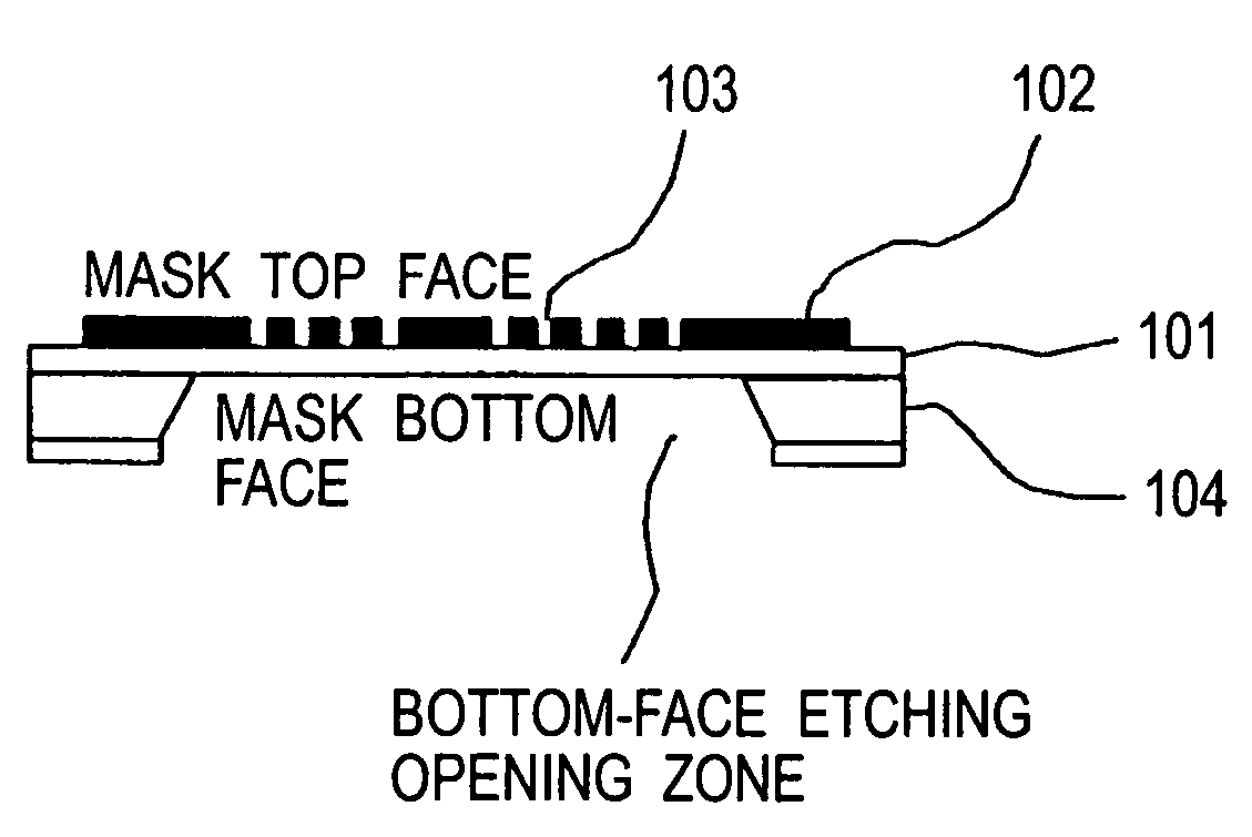
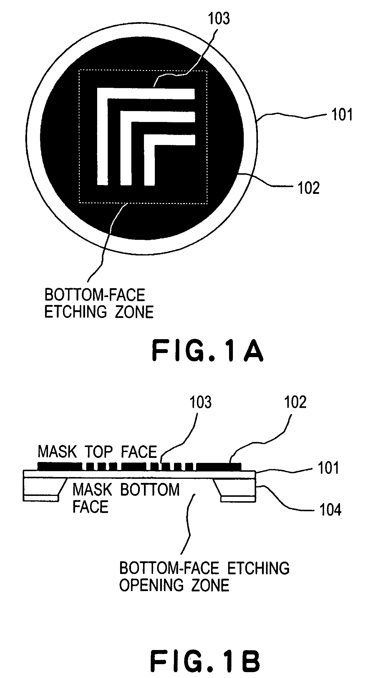
[0032] Referring to FIGS. 1A and 1B, the structure and function of a near-field exposure mask to be used in a near-field exposure method, in an embodiment of the present invention, will be described.

[0033]FIGS. 1A and 1B illustrate the structure of a near-field exposure mask, wherein FIG. 1A is a plan view as seen from a front surface side of the mask, and FIG. 1B is a sectional view.

[0034] As shown in FIGS. 1A and 1B, the near-field exposure mask comprises a mask base material 101 which is provided by a thin film of a film thickness of 0.1 to 100 μm and which is transparent with respect to light of the exposure wavelength. A metal thin film 102 of a film thickness of about 50-100 nm, that constitutes a light blocking film, is provided on the mask base material 101. The metal thin film 102 is formed with a fine opening pattern 103 of a width not greater than 100 nm. The mask base material 101 is supported by a substrate 104.

[0035] If the thickness of the mask base material 101 is...


PUM


Abstract

Disclosed is an exposure method and apparatus, an exposure mask and a device manufacturing method, wherein a first surface of a light blocking member having a plurality of openings formed in a mutually adjoining relation is placed at an exposure object side, and light is projected to the light blocking member from its second surface side so that exposure of the exposure object is carried out on the basis of near field light leaking from the openings. For exposure, interference is caused between surface plasmon polariton waves passing respectively through adjacent openings and going around to the first surface side, and, on the basis of it, a portion having a decreased light intensity is produced in the exposure object so that the exposure is carried out by use of the decreased light intensity portion.

Description

TECHNICAL FIELD [0001] This invention relates to an exposure method and apparatus, an exposure mask, and a device manufacturing method. BACKGROUND ART [0002] Increasing capacity of a semiconductor memory and increasing speed and density of a CPU processor have inevitably necessitated further improvements in fineness of microprocessing through optical lithography. Generally, the limit of microprocessing with an optical lithographic apparatus is of an order of the wavelength of light used. Thus, the wavelength of light used in optical lithographic apparatuses haven been shortened more and more. Currently, near ultraviolet laser is used, and microprocessing of 0.1 μm order is enabled. While the fineness is being improved in the optical lithography, in order to assure microprocessing of 0.1 μm or narrower, there still remain many unsolved problems such as further shortening of laser, development of lenses usable in such wavelength region, and the like. [0003] On the other hand, as a mea...

Claims


Application Information

Patent Timeline
IPC IPC(8): G03C5/00G03B27/42G03F1/00G03F1/70G03F7/20H01L21/027
CPCB82Y10/00G03F1/14G03F7/2014G03F7/70325G03F1/50
Inventor KURODA, RYOMIZUTANI, NATSUHIKOYAMADA, TOMOHIRO
Owner CANON KK
Why Eureka
Try Eureka