A damascene copper wiring image sensor

Active Publication Date: 2006-06-01
SMARTSENS TECH (HK) CO LTD
View PDF15 Cites 180 Cited by
  • Summary
  • Abstract
  • Description
  • Claims
  • Application Information

AI Technical Summary

Benefits of technology

[0024] In alternate embodiments, prior to depositing the refill dielectric, a layer of either reflective or absorptive material may be formed along the side

Problems solved by technology

However, none of these state of the art devices described utilize Copper metallization layers in the pixel design.
Thus, the sensitivity of the CMOS imager pixel is compromised.
That is, S

Method used


Image

  • A damascene copper wiring image sensor
  • A damascene copper wiring image sensor
  • A damascene copper wiring image sensor

Examples


Embodiment Construction

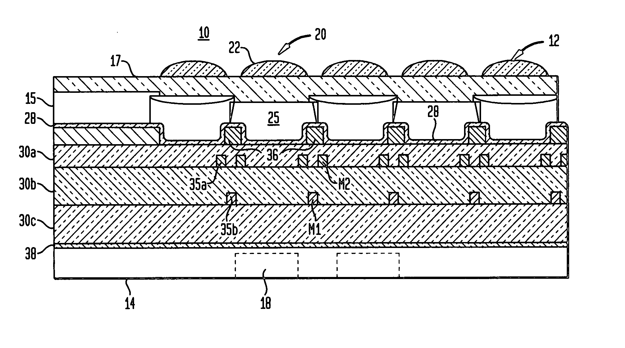
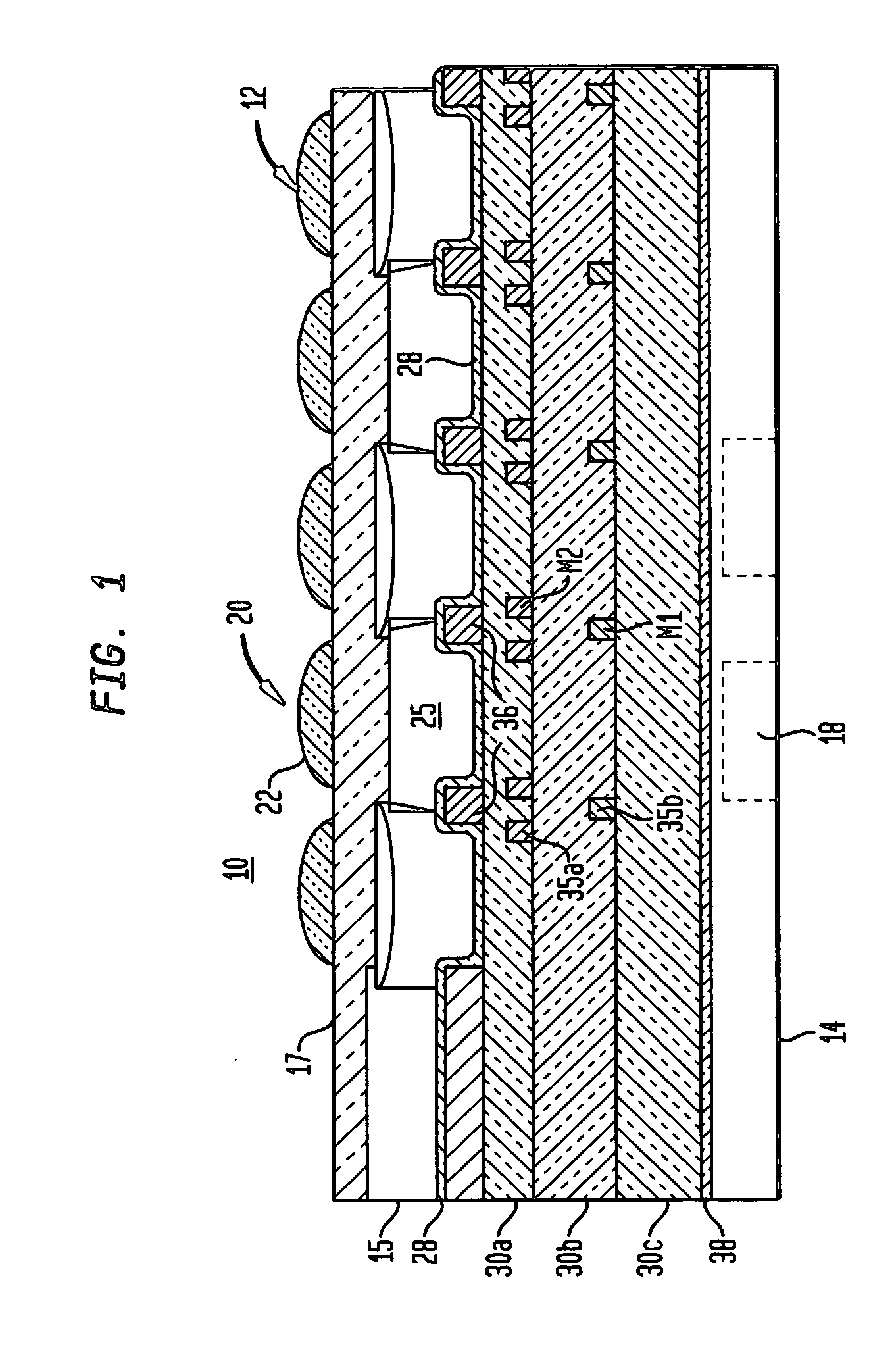
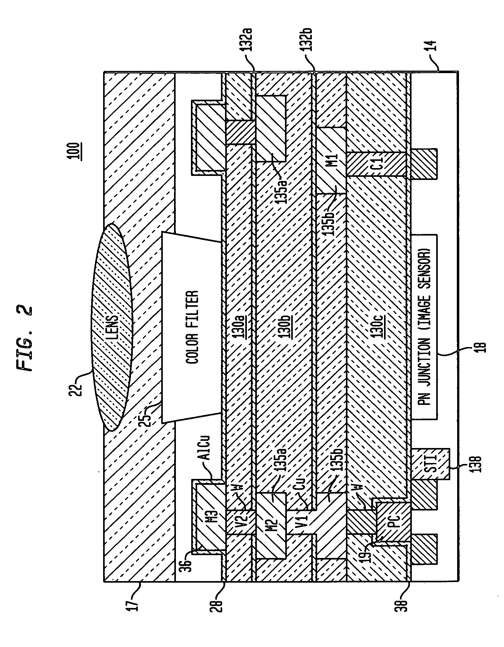
[0037]FIG. 1 depicts image sensor pixel array 10. As shown, the array comprises a plurality of microlenses 12, each having a hemisphere shape, arranged on a smooth planarization layer 17, e.g., a spin on polymer, that is formed on top of a color filter array 15 enabling formation of the microlens array. The color filter array 15 includes individual red, green and blue filter elements 25 (primary color filters) or alternately, cyan, magenta and yellow filter elements (complementary color filter). Each microlens 22 of the microlens array 12 is aligned with a corresponding color filter element 25 and comprises an upper light receiving portion of a pixel 20. The pixel 20 includes a cell portion fabricated upon a semiconductor substrate 14 portion including a stack of comprising one or more interlevel dielectric layers 30a-30c incorporating metallization interconnect levels M1, M2 Aluminum (Al) wire layers 35a, 35b. Interlevel dielectric materials may comprise a polymer or SiO2, for exam...


PUM


Abstract

An image sensor array and method of fabrication wherein the sensor includes Copper (Cu) metallization levels allowing for incorporation of a thinner interlevel dielectric stack with improved thickness uniformity to result in a pixel array exhibiting increased light sensitivity. In the sensor array, each Cu metallization level includes a Cu metal wire structure formed at locations between each array pixel and, a barrier material layer is formed on top each Cu metal wire structure that traverses the pixel optical path. By implementing a single mask or self-aligned mask methodology, a single etch is conducted to completely remove the interlevel dielectric and barrier layers that traverse the optical path. The etched opening is then refilled with dielectric material. Prior to depositing the refill dielectric, a layer of either reflective or absorptive material is formed along the sidewalls of the etched opening to improve sensitivity of the pixels by either reflecting light to the underlying photodiode or by eliminating light reflections.

Description


Claims


Application Information

Patent Timeline
Owner SMARTSENS TECH (HK) CO LTD
Why Eureka
Try Eureka