D/A converter, and A/D converter and signal converter using the same

Inactive Publication Date: 2006-06-01
PANASONIC CORP
View PDF4 Cites 7 Cited by
  • Summary
  • Abstract
  • Description
  • Claims
  • Application Information

AI Technical Summary

Benefits of technology

[0028] It is an object of the present invention to provide a D / A converter having an excellent differential linearity, without adding a correction circuit even in a high-resolution D / A converter with an increased number of bits, and an A / D converter and a signal converter using the same.
[0029] According to the present invention, a D / A conversion is performed in two or more steps using two or more current output type D / A converters. For example, in a first step, upper bits are D / A converted using the current segment manner, while in a second step; lower bits are D / A converted by a shunt current. At the D / A conversion performed in the second step, there is employed a method in which one of the currents generated in the first step is selected, and by shunting a current using the selected current as a reference current, the D / A conversion is then performed, and the current generated in the second step and the current generated in the first step are added each other, thereby generating an output current corresponding to digital data. As a result of this, the D / A conversion having the excellent differential linearity may be performed.
[0036] By implementing the aspects of the present invention, even when a current error occurs due to the variation in resistance caused by the manufacturing variability, occurrences of the differential linearity error can be reduced. Especially, when the high-resolution D / A conversion is performed using R-2R resistors, the current error due to the variation in resistance is significant, but the D / A conversion with the small differential linearity error can be achieved by applying the present invention.

Problems solved by technology

The conventional D / A converter, however, has had two problems to be solved.
The attempt to increase the manufacturing accuracy for the transistors will necessarily result in an increase in size of the transistor Q211.
As a result, the pattern layout configuration has been increased, while producing an irregular shape, so that the conventional D / A converter has had a problem that the optimization has been difficult.
The current variation produced by a change in resistance value of the resistor R caused by the manufacturing variability, however, could not be prevented.
The change in characteristics caused by the variation in the resistance value of the resistor R has been a significant issue in the D / A converter, especially in the high-resolution D / A converter with a large bit number.
As a result, when the D / A converter has had the characteristics to generate the step height as shown in FIG. 12, there has been a problem that the current outputted to the laser diode 2 has been unstable due to the oscillation.
The errors produced in the current flowing through the D / A converter by the R-2R resistor and the current flowing through the segment type D / A converter will cause the differential linearity error during the D / A conversion.
The method described in Patent Document 2, however, has not been able to prevent the differential linearity error due to the current error generated between the respective segments.
Even by the method, however, the generation of the differential linearity error due to the error of the current mirror has not been able to be reduced.
In a signal processing apparatus, which drives the laser diode with the current, there has been a problem that when the step height (differential linearity error) has been generated during the D / A conversion, the laser output has been unstable due to the oscillation in setting a laser intensity.
Meanwhile, also in the comparison type A / D converter using the D / A converter, if there is the differential linearity error in the D / A conversion section, the error is generated during the digital conversion, so that a D / A converter having the small differential linearity error will be required.

Method used


Image

  • D/A converter, and A/D converter and signal converter using the same
  • D/A converter, and A/D converter and signal converter using the same
  • D/A converter, and A/D converter and signal converter using the same

Examples


first embodiment

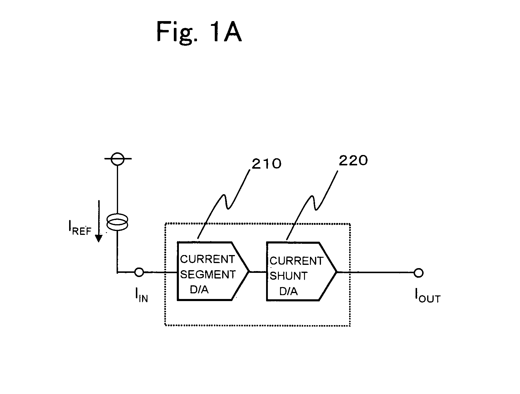
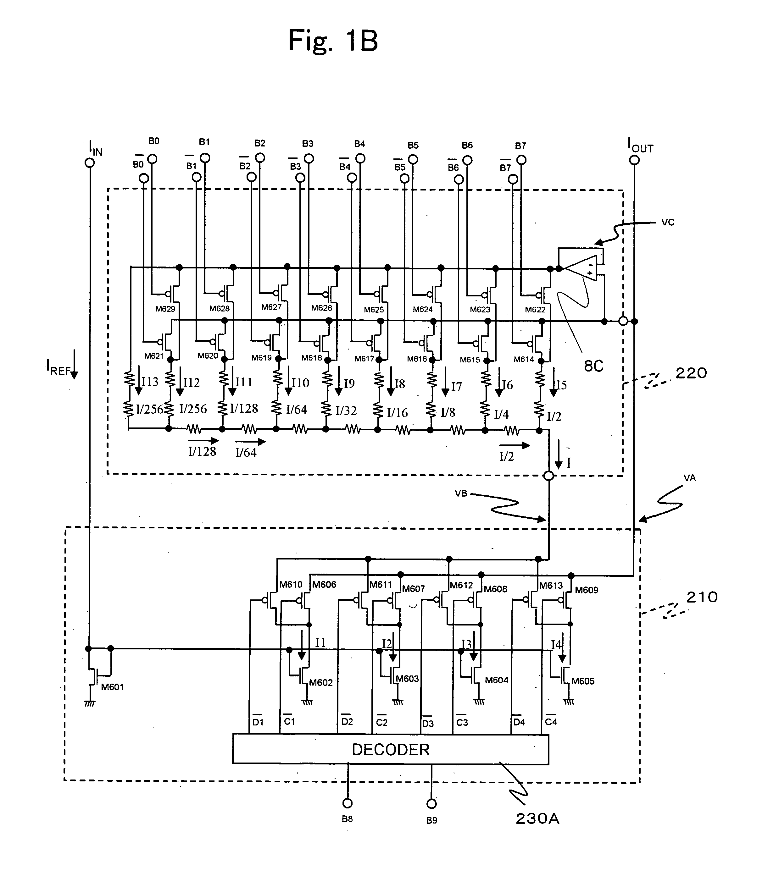
[0061]FIGS. 1A and 1B show a D / A converter according to a first embodiment of the present invention. This first embodiment is obtained by applying the present invention to the D / A converter shown in FIG. 10. FIG. 1A shows a schematic circuit diagram of the D / A converter according to a first embodiment of the present invention, while FIG. 1B shows a specific circuit diagram thereof.

[0062] This D / A converter performs a 10-bit D / A conversion. In FIG. 1B, symbols B0 through B9 represent digital input codes to be converted, in which symbols B9 is an input signal corresponding to MSB (Most Significant Bit) and symbol B0 is an input signal corresponding to LSB (Least Significant Bit) Symbol “−” on the top of symbols B9 through B0 means an inversion thereof.

[0063] According to the first embodiment shown in FIGS. 1A and 1B, upper 2 bits (B9, B8) of the digital input code, namely, digital data to be converted, are D / A converted using a current segment manner, while remaining lower 8 bits (B...

second embodiment

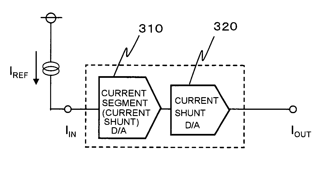
[0075]FIGS. 4A and 4B show a D / A converter according to a second embodiment of the present invention. FIG. 4A shows a schematic circuit diagram of the D / A converter according to the second embodiment of the present invention, while FIG. 4B shows a specific circuit diagram thereof.

[0076] According to the embodiment shown in FIGS. 4A and 4B, the upper 2 bits (B9, B8) are D / A converted using the current segment manner utilizing the shunt currents, while the remaining lower 8 bits (B7 through B0) are D / A converted using the currents shunt by the R-2R resistors.

[0077] Symbol 310 represents a D / A converter block for performing the D / A conversion using the current segment manner to the upper 2 bits. Symbol 320 represents a D / A converter block for D / A converting the lower 8 bits using the currents shunt by the R-2R resistors.

[0078] A voltage of a voltage source V901 shown in FIG. 4B is an arbitrary fixed voltage, and is set within a voltage range for a transistor M913 to exhibit saturate...

third embodiment

[0083] This third embodiment is characterized by using a D / A converter block 420 by the shunt currents shown in FIGS. 6A and 6B instead of the D / A converter blocks 220 and 320 composed of the R-2R resistor section according to the first and second embodiments. The other configuration is the same as that of the first and second embodiments. FIG. 6A shows a schematic circuit diagram of the D / A converter block 420 according to the third embodiment of the present invention, while FIG. 6B shows a specific circuit diagram of the D / A converter block 420 thereof. In FIG. 6B, symbols R1 through R255 represent resistors having the same resistance value. Symbol 430C represents a decoder. Symbol 8C represents a differential amplifier composing the voltage follower and has a similar function to that of the foregoing embodiments.

[0084] A configuration of the decoder 430C is shown in FIGS. 7A and 7B. FIG. 7A shows a circuit diagram of the decoder 430C, while FIG. 7B shows a truth table of the dec...


PUM


Abstract

A current summing type D / A converter having a configuration of two or more steps is provided. In a D / A converter block of the first step, by adding current segments, upper bits are D / A converted, and one of the current segments in the first step is further supplied to a D / A converter block in a second step to be shunt by the D / A converter block in the second step, so that lower bits are D / A converted. The output current in the first step and the output current in the second step are then added each other. According to the foregoing method, the D / A conversion may be performed without causing a differential linearity error.

Description

BACKGROUND OF THE INVENTION [0001] 1. Field of the Invention [0002] The present invention relates to a current summing type D / A (digital to analog) converter, an A / D (analog to digital) converter using the D / A converter, and a signal converter including the D / A converter or the A / D converter. [0003] 2. Description of the Related Art [0004] There exists a semiconductor integrated circuit, which incorporates a large number of D / A (digital to analog) converters to perform signal processing. To achieve high accurate performance has been strongly required particularly to the D / A converter, and the resolution of the D / A converter has been improved by increasing the number of bits in a digital signal. [0005]FIG. 10 is an example showing a signal converter, i.e., a laser output unit. In this signal converter, a current is provided to a laser diode (LD) to be emitted, and by adjusting a current value of the LD using the D / A converter, the laser diode is controlled so as to provide an optimum...

Claims


Application Information

Patent Timeline
IPC IPC(8): H03M1/12
CPCH03M1/687H03M1/747H03M1/785
Inventor OHMI, KAZUYUKITATEHARA, KENICHI
Owner PANASONIC CORP
Why Eureka
Try Eureka