Method for fabricating semiconductor package having conductive bumps on chip

a technology of conductive bumps and semiconductor packages, which is applied in the direction of semiconductor devices, semiconductor/solid-state device details, electrical apparatus, etc., can solve the problems of reducing and affecting the quality of semiconductor packages. , to achieve the effect of improving the production yield and reliability of semiconductor packages, simplifying fabrication processes, and reducing fabrication costs

Inactive Publication Date: 2006-06-08
SILICONWARE PRECISION IND CO LTD
View PDF10 Cites 6 Cited by
  • Summary
  • Abstract
  • Description
  • Claims
  • Application Information

AI Technical Summary

Benefits of technology

[0008] An objective of the present invention is to provide a semiconductor package having conductive bumps on a chip and a method for fabricating the semiconductor package, having a plurality of the conductive bumps respectively formed on bond pads of the chip so as to allow easy positional recognition of the bond pads and assure electrical connection between the bond pads and conductive traces, thereby improving production yield and reliability of the semiconductor package.
[0009] Another objective of the present invention is to provide a semiconductor package having conductive bumps on a chip and a method for fabricating the semiconductor package, not having to deposit a dielectric layer directly on the chip and use a laser drilling technique to form vias through the dielectric layer, thereby reducing fabrication costs and simplifying fabrication processes.
[0010] A further objective of the present invention is to provide a semiconductor package having conductive bumps on a chip and a method for fabricating the semiconductor package, not having to coat a dielectric layer directly on the chip and an encapsulation body encapsulating the chip, thereby preventing delamination at interface between the dielectric layer and the chip or encapsulation body due to CTE (coefficient of the thermal expansion) mismatch.
[0013] The above semiconductor package according to the invention first implants a plurality of conductive bumps on bond pads of the chip and then forms an encapsulation body which encapsulates the chip and conductive bumps whose ends are adapted to be exposed outside of the encapsulation body, so as to allow build-up layers to be subsequently formed on the exposed ends of the conductive bumps. This semiconductor package yields significant benefits. The exposed ends of the conductive bumps allow easy position recognition of the bond pads of the chip, such that conductive traces subsequently formed on the encapsulation body can be well electrically connected to the bond pads through the conductive bumps, thereby improving the production yield and reliability of the semiconductor package. Therefore, compared to the prior art coating a dielectric layer on a chip and an encapsulation body encapsulating the chip and using a laser drilling technique to form a plurality of vias through the dielectric layer for exposing bond pads of the chip, the semiconductor package according to the invention does not require the dielectric layer and laser drilling technique, thereby reducing fabrication costs and simplifying fabrication processes. In the invention, the bond pads of the chip are not covered by the dielectric layer, which eliminates the problems that the bond pads, as being hard to accurately recognized in position by laser, cannot be precisely or completely exposed by the vias through the dielectric layer, and thus electrical connection between the bond pads and conductive traces are degraded. Further, there is no dielectric layer applied over the chip and encapsulation body, which eliminates the problem of delamination between the dielectric layer and the chip or encapsulation body due to CTE mismatch.

Problems solved by technology

The above CSP structure, however, is defective in that the use of RDL technique or the arrangement of conductive traces is limited in accordance with the chip size or area of the active surface of the chip.
Especially with increase in the chip integration and reduction of the chip size, the chip usually cannot provide sufficient surface area for accommodating relatively more solder balls desirably required for the external electrical connection.
However, a significant drawback incurred by the above package structure is that when the laser drilling technique is employed to form vias through the first dielectric layer for exposing the bond pads on the chip, the bond pads covered by the first dielectric layer cannot be easily and precisely recognized by laser in position, making the vias not able to accurately correspond to the positions of the bond pads.
As a result, the bond pads on the chip fail to be completely exposed, and electrical connection between the conductive traces and the incompletely-exposed bond pads is degraded, thereby damaging yield and reliability of the fabricated packages.
Moreover, the provision of first dielectric layer on the chip and encapsulation body and the use of laser drilling technique would undesirably increase fabrication costs and process complexity.
Besides, since the first dielectric layer has a different coefficient of thermal expansion (CTE) from the chip and encapsulation body, under a high temperature environment or in a thermal cycle, delamination may easily occur at interface between the first dielectric layer and the chip or encapsulation body due to different thermal stresses produced therefrom, making the quality and reliability of the fabricated products degraded.

Method used


Image

  • Method for fabricating semiconductor package having conductive bumps on chip
  • Method for fabricating semiconductor package having conductive bumps on chip
  • Method for fabricating semiconductor package having conductive bumps on chip

Examples


first preferred embodiment

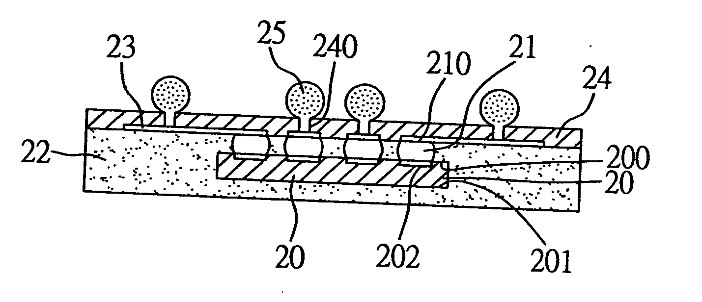
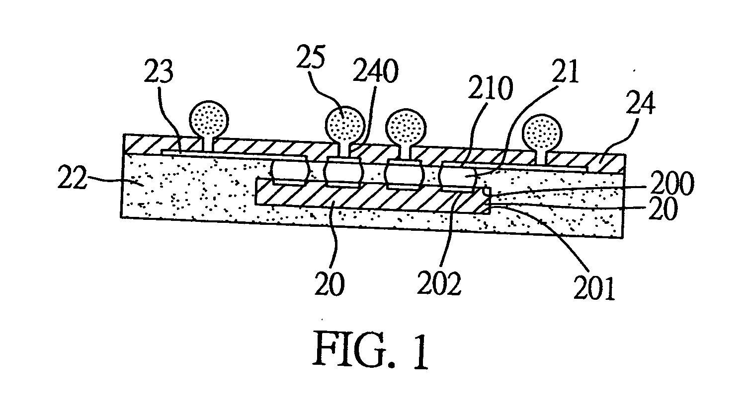
[0022] As shown in FIG. 1, the semiconductor package according to the invention comprises: at least one chip 20 having an active surface 200 and an opposite inactive surface 201, and having a plurality of bond pads 202 formed on the active surface 200; a plurality of conductive bumps 21 respectively formed on the bond pads 202 of the chip 20; an encapsulation body 22 for encapsulating the chip 20 and the conductive bumps 21, wherein ends 210 of the conductive bumps 21 are exposed outside of the encapsulation body 22; a plurality of conductive traces 23 formed on the encapsulation body 22 and electrically connected to the exposed ends 210 of the conductive bumps 21; a solder mask layer 24 applied over the conductive traces 23 and having a plurality of openings 240 for exposing predetermined portions of the conductive traces 23; and a plurality of solder balls 25 respectively formed on the exposed portions of the conductive traces 23.

[0023] The above semiconductor package can be fabr...

second preferred embodiment

[0035]FIG. 3 shows a semiconductor package according to a second preferred embodiment of the invention. As shown, this semiconductor package is structurally similar to that of the first embodiment, with the difference in that during the grinding process of FIG. 2E, besides grinding the surface 220 of the encapsulation body 22 that is flush with the ends 210 of the conductive bumps 21, a portion of the encapsulation body 22 covering the inactive surface 201 of the chip 20 is ground off to allow the inactive surface 201 to be exposed.

[0036] In addition to the improvements achieved by the semiconductor package according to the above first embodiment, the exposed inactive surface 201 of the chip 20 help dissipate heat produced from the chip 20 to an external environment or the atmosphere, thereby enhancing heat dissipating efficiency of the semiconductor package according to this embodiment.

third preferred embodiment

[0037]FIG. 4 shows a semiconductor package according to a third preferred embodiment of the invention. As shown, this semiconductor package is structurally similar to that of the first embodiment, with the difference in that after forming the conductive traces 23 (hereinafter referred to as “first conductive traces”) on the encapsulation body 22, at least one dielectric layer 27 is applied over the first conductive traces 23 and formed with a plurality of vias 270 penetrating through the dielectric layer 27, to allow predetermined portions of the first conductive traces 23 to be exposed by the vias 270. Then, a plurality of second conductive traces 28 are formed on the dielectric layer 27, and each of the second conductive traces 28 is adapted to be electrically connected to at least one of the exposed portions of the first conductive traces 23.

[0038] Afterwards, a solder mask layer 24 is applied over the second conductive traces 28 and formed with a plurality of openings 240 for e...


PUM


Abstract

A semiconductor package having conductive bumps on a chip and a fabrication method thereof are provided. A plurality of the conductive bumps are deposited respectively on bond pads of the chip. An encapsulation body encapsulates the chip and conductive bumps while exposing ends of the conductive bumps. A plurality of conductive traces are formed on the encapsulation body and electrically connected to the exposed ends of the conductive bumps. A solder mask layer is applied over the conductive traces and formed with openings for exposing predetermined portions of the conductive traces. The exposed portions of the conductive traces are connected to a plurality of solder balls respectively. The conductive bumps on the bond pads of the chip allow easy positional recognition of the bond pads, making the conductive traces well electrically connected to the bond pads through the conductive bumps and assuring the quality and reliability of the semiconductor package.

Description

FIELD OF THE INVENTION [0001] The present invention relates to semiconductor packages and fabrication methods thereof, and more particularly, to a semiconductor package not having a chip carrier, and a method for fabricating the semiconductor package. BACKGROUND OF THE INVENTION [0002] A semiconductor package is used to accommodate at least one integrated circuit component such as semiconductor chip and preferably made compact in size. To achieve this goal, there is a type of small scale semiconductor package, named chip scale package (CSP), which has a size substantially equal or slightly larger than that of the chip incorporated therein. [0003] U.S. Pat. Nos. 5,892,179, 6,103,552, 6,287,893, 6,350,668 and 6,433,427 disclose a CSP structure which directly fabricates build-up layers on a chip and utilizes a RDL (redistribution layer) technique to redistribute bond pads of the chip to predetermined positions, while not requiring a chip carrier such as substrate or lead frame. As show...

Claims


Application Information

Patent Timeline
Patent Type & Authority Applications(United States)
IPC IPC(8): H01L23/053H01L21/56H01L21/60H01L21/68H01L23/31H01L23/538
CPCH01L21/561H01L2224/12105H01L23/3121H01L23/5389H01L24/19H01L24/96H01L24/97H01L2224/04105H01L2224/16H01L2224/20H01L2224/97H01L2924/01013H01L2924/01029H01L2924/01079H01L2924/01082H01L2924/14H01L2924/15311H01L21/568H01L2224/0401H01L2924/18162H01L2924/01033H01L2224/82H01L2924/351H01L2924/12042H01L2924/00
Inventor HUANG, CHIEN-PINGHSIAO, CHENG-HSU
Owner SILICONWARE PRECISION IND CO LTD
Why Eureka
Try Eureka