Field emission display with electron trajectory field shaping

a field emission display and electron trajectory technology, applied in the manufacture of electrode systems, electric discharge tubes/lamps, discharge tubes luminescnet screens, etc., can solve the problems of increasing the power requirements of the device, unsatisfactory large spot size, and disadvantages of prior art focusing structures

Inactive Publication Date: 2006-06-08
MOTOROLA SOLUTIONS INC
View PDF16 Cites 18 Cited by
  • Summary
  • Abstract
  • Description
  • Claims
  • Application Information

AI Technical Summary

Benefits of technology

[0007] An apparatus is provided for focusing electrons being emitted from a field emission device. The apparatus comprises a substrate having first and second portions, and a cathode metal layer formed over the substrate in the first portion to partially define a sidewall for a trench in the second portion. A ballast layer is formed over the substrate in the second portion, the cathode metal layer, and the sidewall. A first dielectric layer is formed over the ballast layer in the first portion. A gate extraction metal layer is forme...

Problems solved by technology

This separation distance that is sufficient to prevent unwanted electrical events can result in an undesirably large spot size.
Such prior art focusing structures suffer from disadvantages.
For example, the capacitance between the focusing structures and the gate extraction electrodes increases the power requirements of the device.
Many focusing structures add additional layers and processing steps to reduce the beam spot size, and this significantly increases fabrication cost and reduces yield.
Processing geometries are reduced for many methods, thus reducing the available emitter area, increasing the sensitivity to defects, and increasing processing and equipment costs associated with decrease in feature sizes.
The extra sheet adds costs, the precision alignment step reduces yield, and the device requires a double set of spacers, which is extremely complex and costly...

Method used


Image

  • Field emission display with electron trajectory field shaping
  • Field emission display with electron trajectory field shaping
  • Field emission display with electron trajectory field shaping

Examples


first embodiment

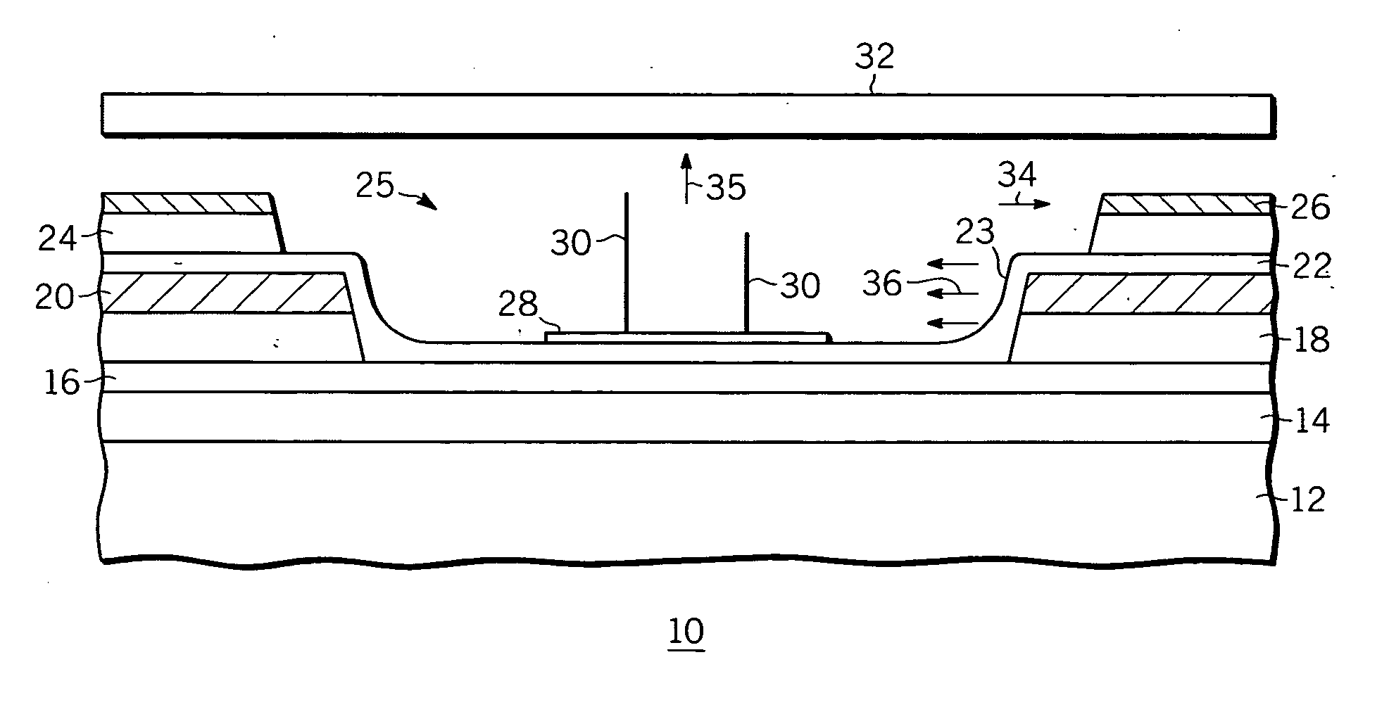
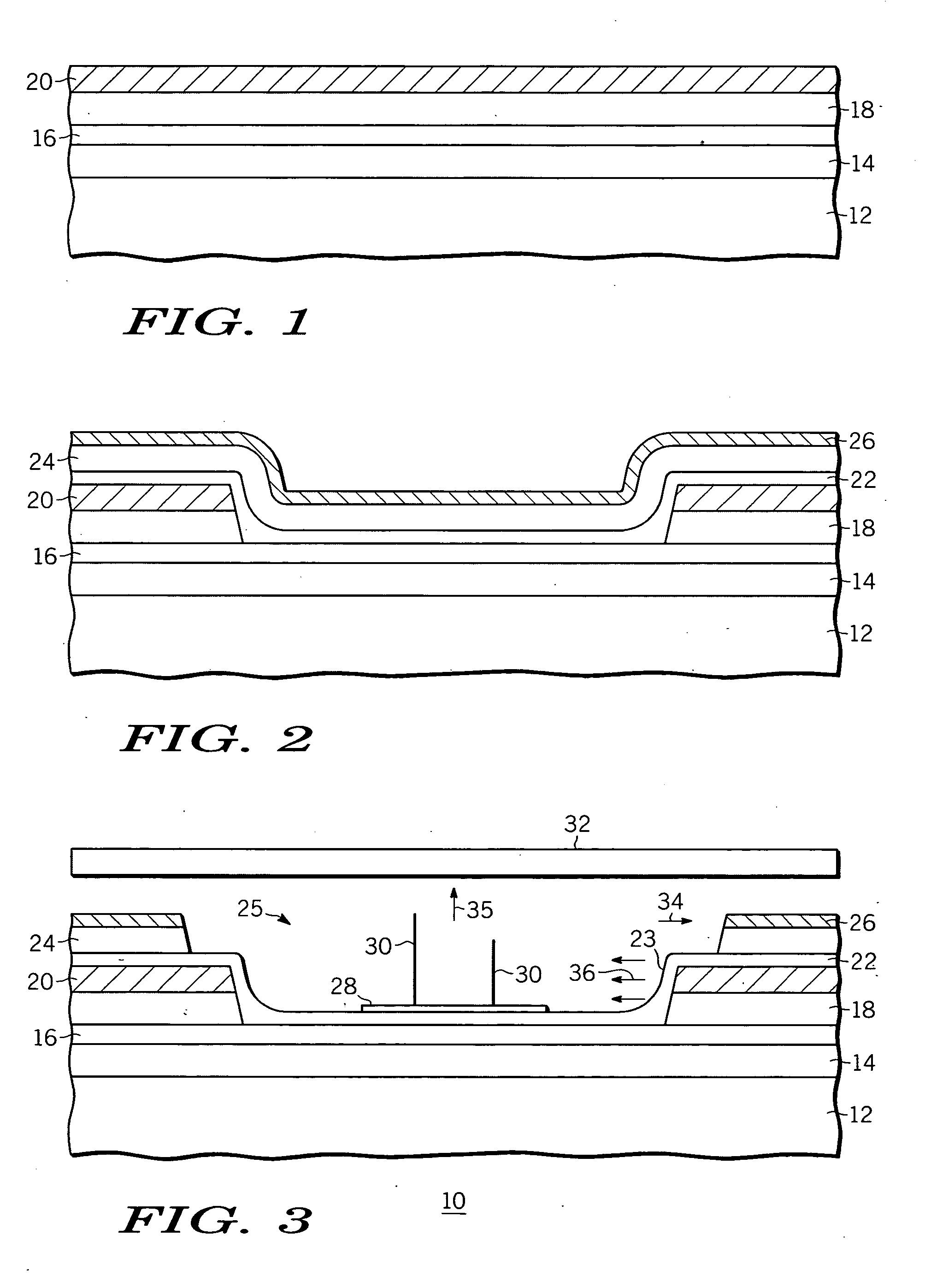
[0014] Referring to FIGS. 1-3, the field emission device 10 according to the present invention includes a dielectric layer 14 deposited on the substrate 12. The substrate 12, for example, comprises glass, silicon, or ceramic. The dielectric layer 14, for example, comprises silicon oxide and would preferably be approximately 1 micron thick. A hard mask 16 of diamond-like carbon or nitride of approximately 0.05-0.5 microns is deposited on the dielectric layer 14 and is used for a self-limiting etch stop to aid in fabrication of a trench structure. Another dielectric layer 18 of silicon oxide and approximately 0.1-2.0 microns thick is deposited on the hard mask 16. A metal layer 20 of molybdenum or copper, for example, and of sufficient thickness to limit the voltage drop over the length of the cathode metal, approximately 0.2-2 microns thick, is deposited on the dielectric layer 18.

[0015] Referring to FIG. 2, a photo etch is performed on the metal 20 and then on the dielectric 18 in a...

second embodiment

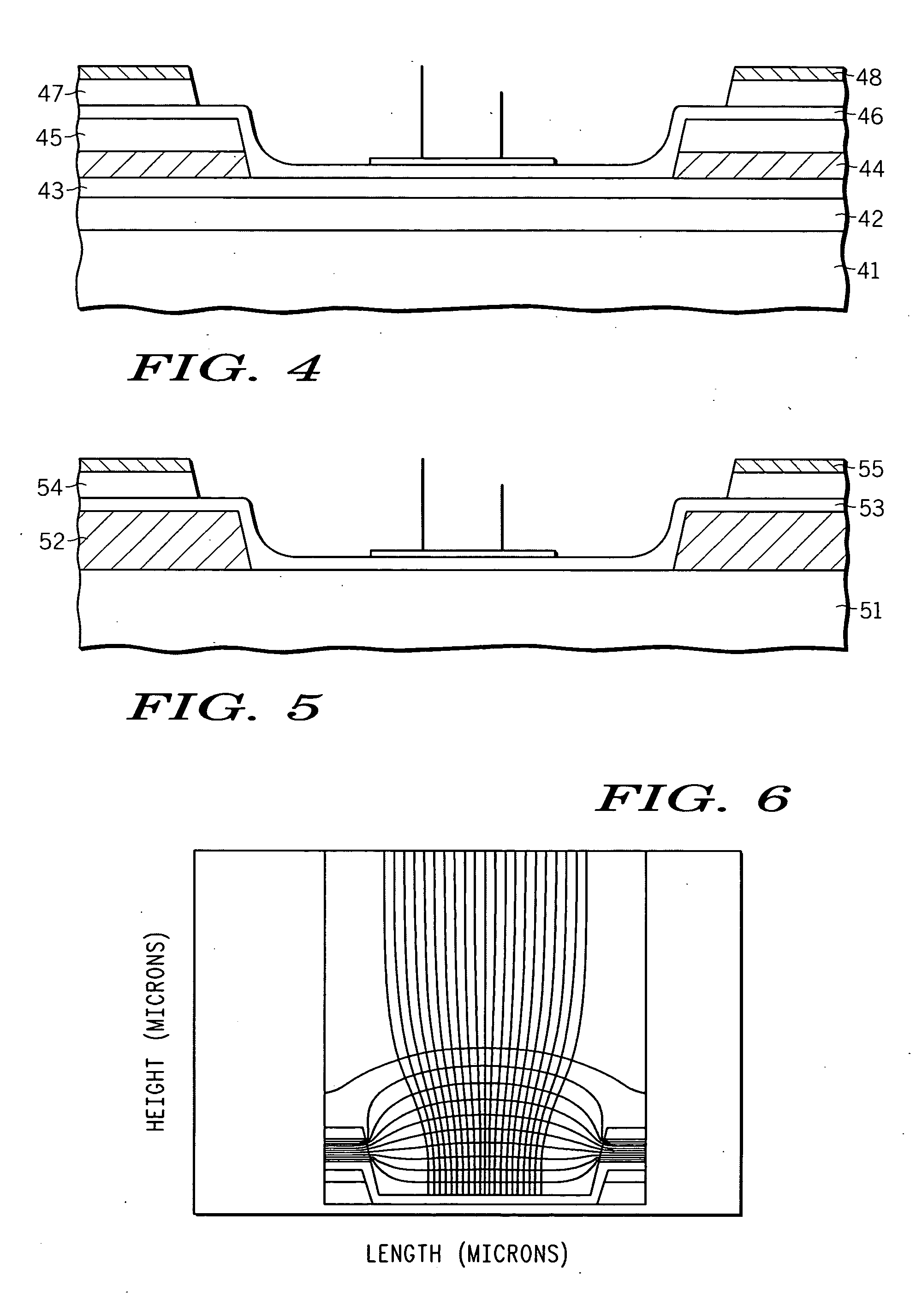
[0020] In a second embodiment, shown in FIG. 4, the first set of layers is ordered with cathode metal 44 on the bottom, a dielectric layer 45 in the middle, and the ballast layer 46 on top. A typical fabrication sequence would involve providing a substrate 41 with a barrier layers 42 deposited thereover (for example SiO2 or SiN), depositing a cathode metal layer 44, depositing a dielectric layer 45, depositing a photoresist, patterning and developing the photoresist, etching the dielectric layer 45 and then the cathode metal layer 44. The ballast layer 46 is deposited as the top layer, thereby covering the sidewall, and a dielectric layer 47 and a gate layer 48 are formed thereon. It is not patterned in the vicinity of the trench. The ballast sidewall height is desired to be at most 2× the emitter height, less the catalyst thickness. Emitters greater than 1.5× the total trench depth risk contacting the gate prior to biasing and becoming attached by Van der Waal's forces. The catalys...

third embodiment

[0021] In a third embodiment, shown in FIG. 5, the first set of layers is ordered with a thick cathode metal 52 on the bottom, and the ballast layer 53 on top. A dielectric layer is not used. A typical fabrication sequence would involve providing a substrate 51 with barrier layers on it of, for example, SiO2 or SiN, depositing a thick cathode metal layer 52, depositing a photoresist, patterning and developing the photoresist, etching the cathode metal layer 52. The ballast is deposited as the top layer, thereby covering the sidewall, and a dielectric layer 54 and a gate extraction layer 55 are formed thereon. The ballast sidewall height is desired to be at most 2× the emitter height, less the catalyst thickness.

[0022] This invention, in addition to focusing the electrons, also aligns the nanotubes perpendicular to the electric field lines. The presence of the sidewall layer 23 at near the cathode 20 potential directs the electric field lines to be more parallel to the substrate 12. ...


PUM


Abstract

An apparatus is provided for focusing electrons being emitted from a field emission device. The apparatus comprises a substrate (12,41,51) having first and second portions, and a cathode metal layer (20,44,52) formed over the substrate (12,41,51) in the first portion to partially define a sidewall (23) for a trench (25) in the second portion. A ballast layer (22,46,53) is formed over the substrate (12,41,51) in the second portion, the cathode metal layer (20,44,52), and the sidewall (23). A first dielectric layer (24,47,54) is formed over the ballast layer (22,46,53) in the first portion. A gate extraction metal layer (26,48,55) is formed over the first dielectric layer. At least one emitter (30) comprising a high aspect ratio conductive material is formed above the substrate and in the trench (25) having a sidewall (23) defined by the first dielectric layer (24,47,54) and the cathode metal layer (20,44,52). The ballast layer (22,46,53) extends along the sidewall and conductively contacts the cathode metal layer and the at least one emitter. An anode (32) is positioned to receive electrons from the at least one emitter (30). The ballast layer (22,46,53) provides a force that counteracts the sidewise pull of the gate extraction metal layer (26,48,55).

Description

FIELD OF THE INVENTION [0001] The present invention generally relates to field emission displays and more particularly to a field emission display structure that focuses the electrons from the emitter. BACKGROUND OF THE INVENTION [0002] Field emission devices that generate electron beams from electron emitters such as carbon nanotubes at an anode plate are well known in the art. Each of the electron beams are received at a spot on the anode plate and define a corresponding spot size. The separation distance between the cathode plate and the anode plate determine, in part, the spot size. It is known in the art to control the spot size by using focusing structures to collimate the electron beams. [0003] To achieve adequate display brightness, the anode should be maintained at a high voltage relative to the cathode. Consequently, the anode plate and cathode plate should be spaced far enough apart that nanotubes due not emit electrons from the anode field alone, and the spacers that sep...

Claims


Application Information

Patent Timeline
IPC IPC(8): H01J63/04H01J1/62
CPCB82Y10/00H01J3/022
Inventor HOWARD, EMMETT M.DEAN, KENNETH A.JOHNSON, MICHAEL R.
Owner MOTOROLA SOLUTIONS INC
Why Eureka
Try Eureka