
Apparatus for generating plasma by RF power

Inactive Publication Date: 2006-06-22
APPLIED MATERIALS INC
View PDF60 Cites 278 Cited by
  • Summary
  • Abstract
  • Description
  • Claims
  • Application Information

AI Technical Summary

Problems solved by technology

Native oxides may also result when the substrate surface is contaminated by etching.
Oxygen exposure typically forms a thin native oxide film, such as between 5 and 20 angstroms, sufficient to cause difficulties in subsequent fabrication processes.
Such difficulties usually affect the electrical properties of semiconductor devices formed on the substrate.
For example, a particular problem arises when native silicon oxide films are formed on exposed silicon containing layers, especially during processing of Metal Oxide Silicon Field Effect Transistor (“MOSFET”) structures.
Silicon oxide films are electrically insulating and are undesirable at interfaces with contact electrodes or interconnecting electrical pathways because they cause high electrical contact resistance.
Native silicon oxide films at the interface between the substrate and the metal reduce the compositional uniformity of the silicide layer by impeding the diffusion chemical reaction that forms the metal silicide.
This results in lower substrate yields and increased failure rates due to overheating at the electrical contacts.
However, sputter etch processes can damage delicate silicon layers by physical bombardment.
Wet etch processes such as this, however, are disadvantageous in today's smaller devices where the aspect ratio exceeds 4:1, and especially where the aspect ratio exceeds 10:1.
As a result, the removal of the native oxide film is incomplete.
Similarly, a wet etch solution, if successful in penetrating a feature of that size, is even more difficult to remove from the feature once etching is complete.
One disadvantage to using fluorine-containing gases, however, is that fluorine is typically left behind on the substrate surface.
Fluorine atoms or fluorine radicals left behind on the substrate surface detrimentally affect further processing of the substrate.
For various reasons, the fluorine processing sequence and wafer transfer to an anneal chamber is not desirable for cleaning small features.
Namely, wafer throughput is greatly diminished because of the time involved to transfer the wafer.
Also, the wafer is highly susceptible to further oxidation or other contamination during the transfer.
Moreover, the cost of ownership is doubled because two separate chambers are needed to complete the process.

Method used


Image

  • Apparatus for generating plasma by RF power
  • Apparatus for generating plasma by RF power
  • Apparatus for generating plasma by RF power

Examples


Embodiment Construction

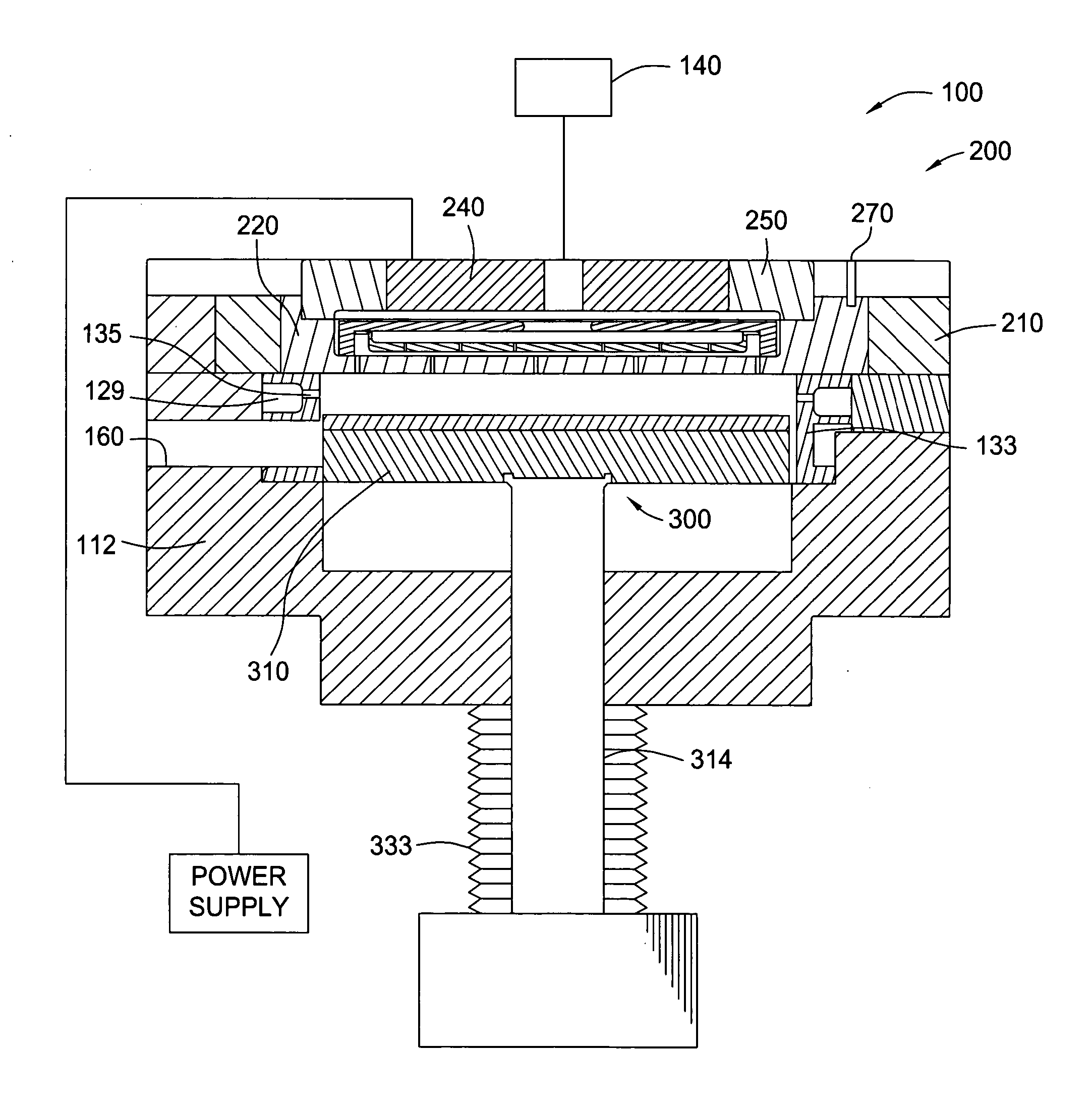
[0019] A processing chamber suitable for a variety of substrate processing methods is provided. An embodiment of the chamber is particularly useful for performing a plasma assisted dry etch process that requires both heating and cooling of the substrate surface without breaking vacuum. For example, the processing chamber described herein is envisioned to be best suited for a front-end-of line (FEOL) clean chamber for removing oxides and other contaminants from a substrate surface.

[0020] A “substrate surface”, as used herein, refers to any substrate surface upon which processing is performed. For example, a substrate surface may include silicon, silicon oxide, doped silicon, germanium, gallium arsenide, glass, sapphire, and any other materials such as metals, metal nitrides, metal alloys, and other conductive materials, depending on the application. A substrate surface may also include dielectric materials such as silicon dioxide, organosilicates, and carbon doped silicon oxides. Th...


PUM

PropertyMeasurementUnit
Surface areaaaaaaaaaaa
Frequencyaaaaaaaaaa
Heataaaaaaaaaa

Abstract

A method and apparatus for processing a substrate is provided. In one aspect, the chamber comprises a chamber body and a support assembly at least partially disposed within the chamber body adapted to support a substrate thereon. The chamber further comprises a lid assembly disposed on an upper surface of the chamber body. The lid assembly includes a top plate and a gas delivery assembly which define a plasma cavity therebetween, wherein the gas delivery assembly is adapted to heat the substrate. A remote plasma source having a U-shaped plasma region is connected to the gas delivery assembly.

Description

CROSS-REFERENCE TO RELATED APPLICATIONS [0001] This application claims benefit of U.S. provisional patent application Ser. No. 60 / 637,897, filed Dec. 21, 2004, which is herein incorporated by reference.BACKGROUND OF THE INVENTION [0002] 1. Field of the Invention [0003] Embodiments of the present invention generally relate to semiconductor processing equipment. More particularly, embodiments of the present invention relate to generating plasma for a chemical vapor deposition (CVD) system or an in situ chamber cleaning system. [0004] 2. Description of the Related Art [0005] A native oxide typically forms when a substrate surface is exposed to oxygen. Oxygen exposure occurs when the substrate is moved between processing chambers at atmospheric conditions, or when a small amount of oxygen remaining in a vacuum chamber contacts the substrate surface. Native oxides may also result when the substrate surface is contaminated by etching. [0006] Oxygen exposure typically forms a thin native o...

Claims


Application Information

Patent Timeline
IPC IPC(8): C23F1/00H01L21/306
CPCH01J37/32082H01J37/32357H01J37/32541H01L21/28247H01L21/31116H01L21/67069H01L29/665
Inventor CHANG, YUTZU, GWO-CHUANUMOTOY, SALVADOR P.KAO, CHIEN-TEHKUANG, WILLIAMYUAN, XIAOXIONGCHANG, MEI
Owner APPLIED MATERIALS INC
Learn More