

Semiconductor device and manufacturing method thereof
a technology of semiconductors and semiconductors, applied in the direction of semiconductor devices, basic electric elements, electrical equipment, etc., can solve the problems of difficult to freely set the breakdown mechanism becomes more complicated than that described, and the value of bvds cannot be controlled with high accuracy
- Summary
- Abstract
- Description
- Claims
- Application Information
AI Technical Summary
Benefits of technology
Problems solved by technology
Method used
Image

Examples
first embodiment
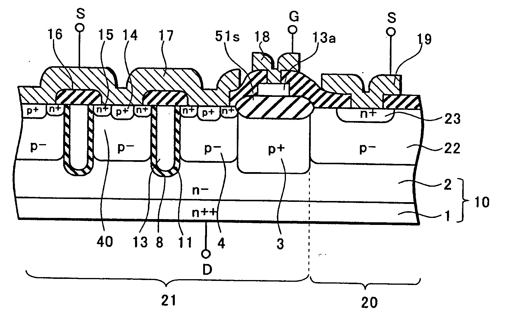
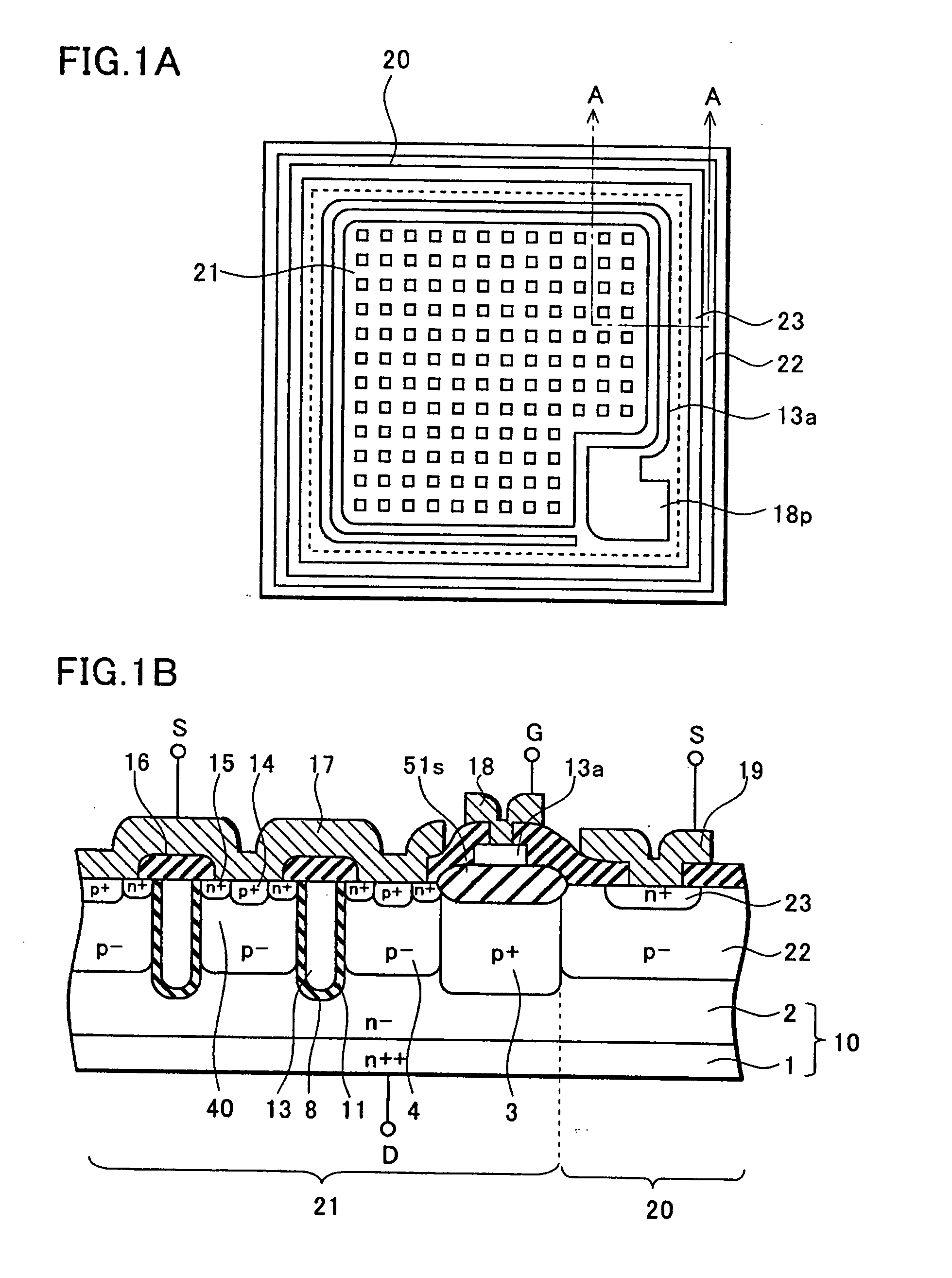
[0039] With reference to FIGS. 1A and 1B, the present invention will be described. FIGS. 1A and 1B show a structure of a semiconductor device according to the embodiment of the present invention. FIG. 1A is a schematic plan view of a chip, in which metal electrode layers such as a source electrode and a gate connection electrode are omitted. Moreover, FIG. 1B is an enlarged cross-sectional view along the line A-A.
[0040] The semiconductor device includes an element part 21 and an element peripheral part 20. In the element part 21 inside the broken line, a number of MOS transistors 40 are arranged. A first source electrode 17 is provided so as to be connected to a source region 15 of each of the MOS transistors 40 on the element part 21.
[0041] A gate electrode 13 of each of the MOS transistors 40 is extended to a peripheral edge of the element part 21 by a connection part 13a. The connection part 13a is connected to a gate pad electrode 18p through a gate connection electrode 18 prov...
second embodiment
[0064] In the second embodiment, a first opposite conductivity type region 24 having an impurity concentration lower than that of a peripheral region 22 is provided in the peripheral region 22.
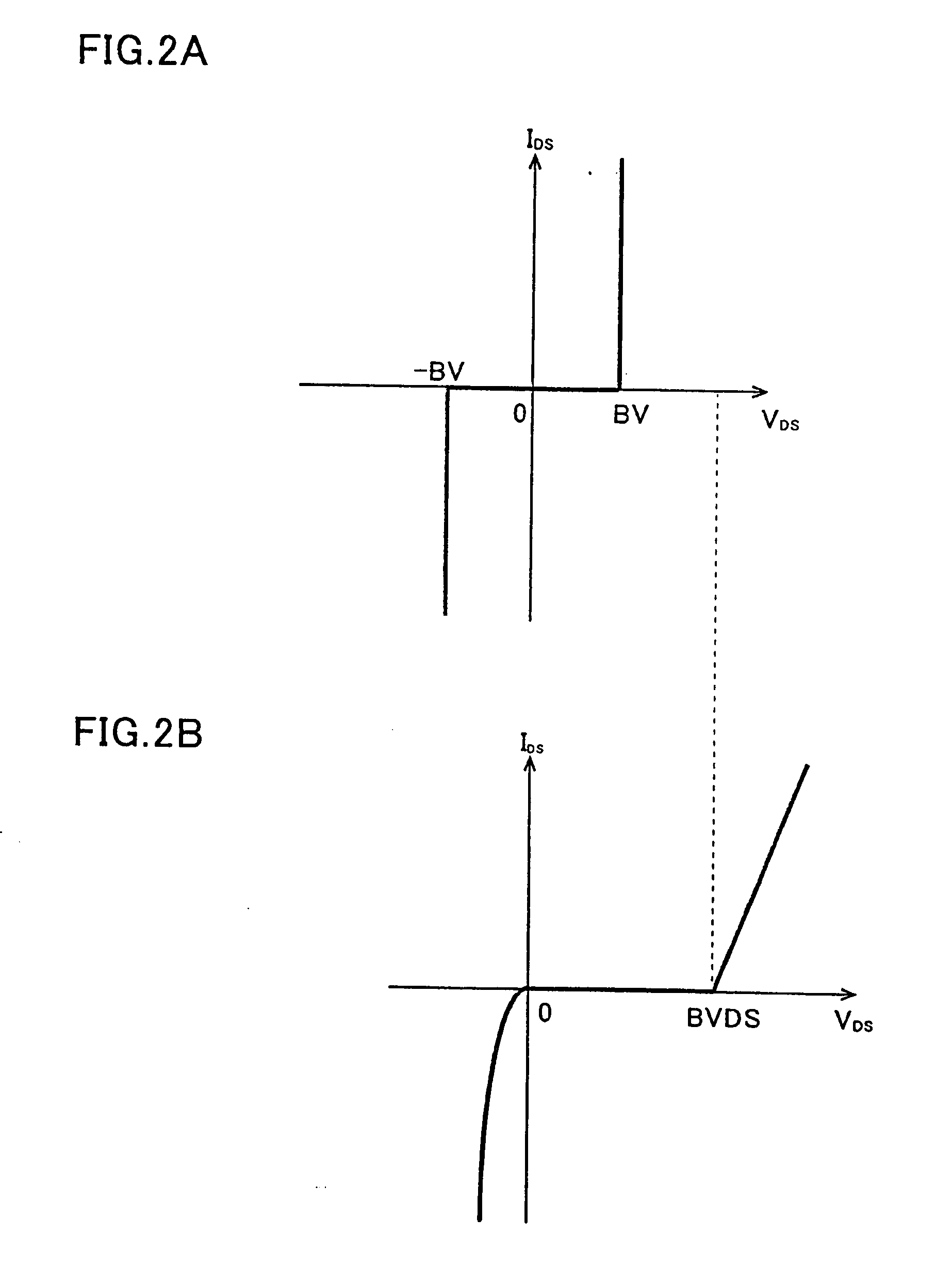
[0065] A breakdown voltage of an npn junction is determined mainly based on an impurity concentration of a p layer. The lower the impurity concentration of the p layer, the more the breakdown voltage increases. Accordingly, in the structure of the first embodiment (FIGS. 1A and 1B), if it is requested to increase the breakdown voltage (BVDS), counter doping is performed to form a first p-type region 24 having a concentration lower (p−−) than that of the peripheral region 22. Thus, the impurity concentration of the p layer in the npn junction is reduced, and the BVDS is increased. Note that, also in this case, the first p-type region 24 has such an impurity concentration as to set the BVDS lower than that of a channel layer 4.
[0066] Also in the second embodiment, the npn junction is formed in ...
third embodiment
[0067]FIG. 4 shows a A plan view is the same as that shown in FIG. 3A, and FIG. 4 shows a cross-sectional view along the line B-B.
[0068] In the third embodiment, a second opposite conductivity type region 34 having an impurity concentration higher than that of a peripheral region 22 is provided in the peripheral region 22.
[0069] In the case where a MOSFET is required to have a breakdown voltage (of 5V or lower) which conforms to an LSI or the case where a MOSFET is desired to have a breakdown voltage of 2 to 3V in accordance with an LSI having a low power supply voltage, a breakdown voltage of an element peripheral part 20 has to be set lower than a breakdown voltage of a gate oxide film.
[0070] In such a case, it is better to provide a second p-type region 34, which has the impurity concentration higher than that of a channel layer 4. Thus, an impurity concentration of a p layer in an npn junction can be increased, and the breakdown voltage of the element peripheral part 20 can b...
PUM
 Abstract
Description
Claims
Application Information