
Semiconductor storage device and semiconductor integrated circuit

a semiconductor integrated circuit and semiconductor technology, applied in semiconductor devices, digital storage, instruments, etc., can solve the problems of being difficult to fabricate dram cells, disrupting normal transistor operation, and unclear how to design logic circuit transistors

Inactive Publication Date: 2006-06-22
KK TOSHIBA
View PDF16 Cites 9 Cited by
  • Summary
  • Abstract
  • Description
  • Claims
  • Application Information

AI Technical Summary

Benefits of technology

The present invention relates to a semiconductor storage device with a logic circuit and a floating body cell (FBC) formed on a substrate. The device includes a first semiconductor layer, a second semiconductor layer, and a third semiconductor layer. The second and third semiconductor layers are set to have different potentials to prevent unwanted coupling between them. The logic circuit is formed on the first semiconductor layer and includes a main gate and an auxiliary gate. The FBC includes a channel body of floating type and a main gate. The device also includes a plurality of polysilicon layers or metal layers formed separate from each other inside the buried insulation film in accordance with the FBC and logic circuit. The technical effects of the invention include improved signal transfer and reduced power consumption.

Problems solved by technology

It is concerned that as a DRAM cell constructed by a conventional one transistor and one capacitor having a trench capacitor and a stacked capacitor is becoming smaller, it is becoming difficult to fabricate the DRAM cell.
However, when the potential of the substrate under a transistor in a peripheral circuit, particularly, a PFET in the peripheral circuit becomes a negative potential, since the buried oxide film is thin, a back channel of the PFET is turned on and it causes a problem such that a normal transistor operation is disturbed.
On the other hand, in the case of forming an FBC on an FD-SOI, it is unclear how to design a transistor of a logic circuit in the case where both a peripheral circuit of a memory and an FBC memory are mounted.
Particularly, when both a P-type FET (PFET) and an N-type FET (NFET) are formed on a very thin silicon film and a substrate voltage is set to 0V in a normal fashion, and the absolute value of the threshold voltage of a PFET of an N-type polysilicon gate is too high, an NFET becomes a depletion type (a field effect transistor having a negative threshold voltage), so that practical use becomes impossible.
Since the threshold voltages change depending on the thickness of a silicon film, in the case of a very thin silicon film, a subtle change in the thickness of the silicon film results in a large change in a threshold voltage, and it causes a problem such that a stable operation of the device is disturbed.

Method used


Image

  • Semiconductor storage device and semiconductor integrated circuit
  • Semiconductor storage device and semiconductor integrated circuit
  • Semiconductor storage device and semiconductor integrated circuit

Examples


first embodiment

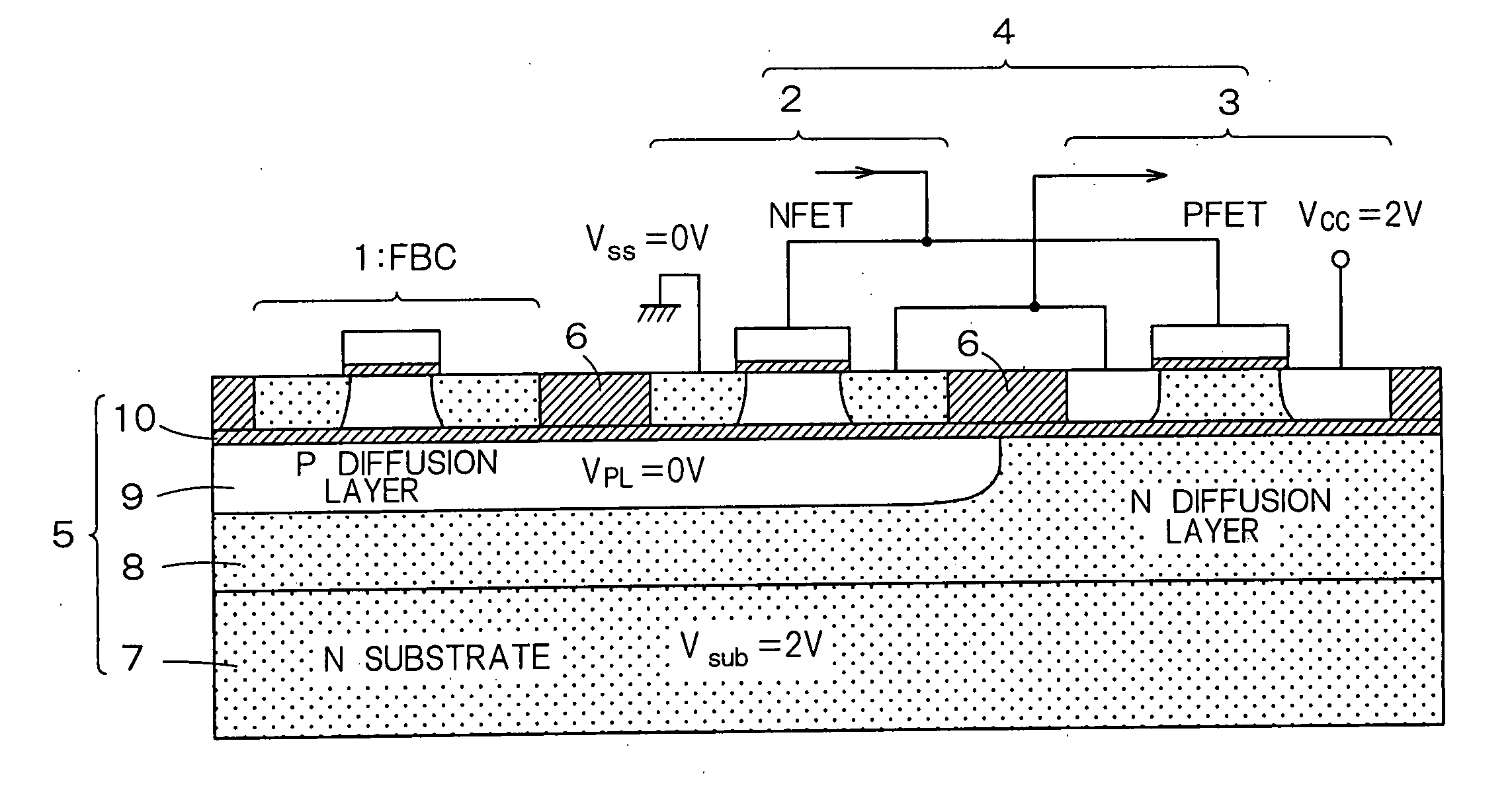
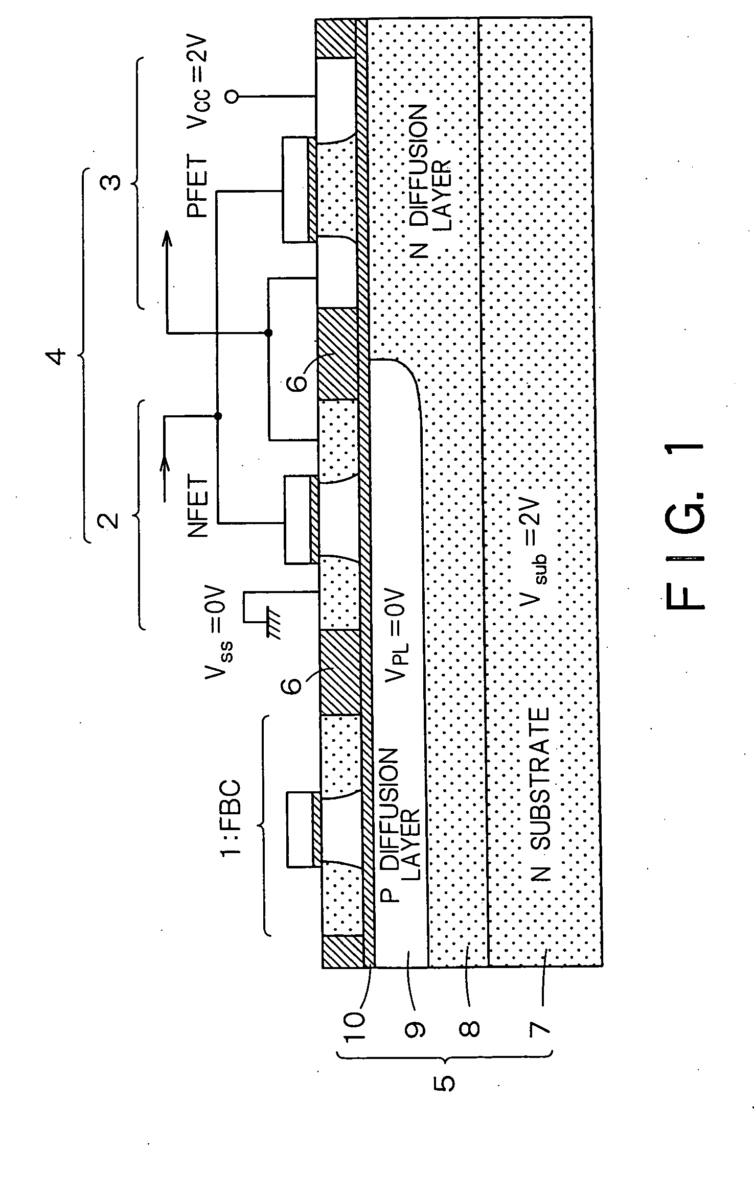
[0071]FIG. 1 is a cross section showing a first embodiment of a semiconductor storage device according to the invention. The semiconductor storage device of FIG. 1 is obtained by forming an FBC (Floating Body Cell) 1 and a peripheral circuit 4 having an N-type MOSFET (hereinbelow, NFET) 2 and a P-type MOSFET (hereinbelow, PFET) 3 so as to be isolated from each other by an insulation layer 6 on a partially depleted SOI (Silicon On Insulator) board 5.

[0072] The SOI board 5 has an N-type diffusion layer 8 formed on an N-type silicon wafer (N wafer) 7, a P-type diffusion layer 9 formed in a part of the N diffusion layer 8, and a thin buried oxide film 10 formed on the top faces of the N diffusion layer 8 and the P diffusion layer 9. On the top face of the buried oxide film 10, the FBC 1, NFET 2, and PFET 3 are formed.

[0073] The P diffusion layer 9 is formed below the FBC 1 and the NFET 2. The potentials Vsub of the N wafer 7 and the N diffusion layer 8 are equal to 2V, and the potenti...

second embodiment

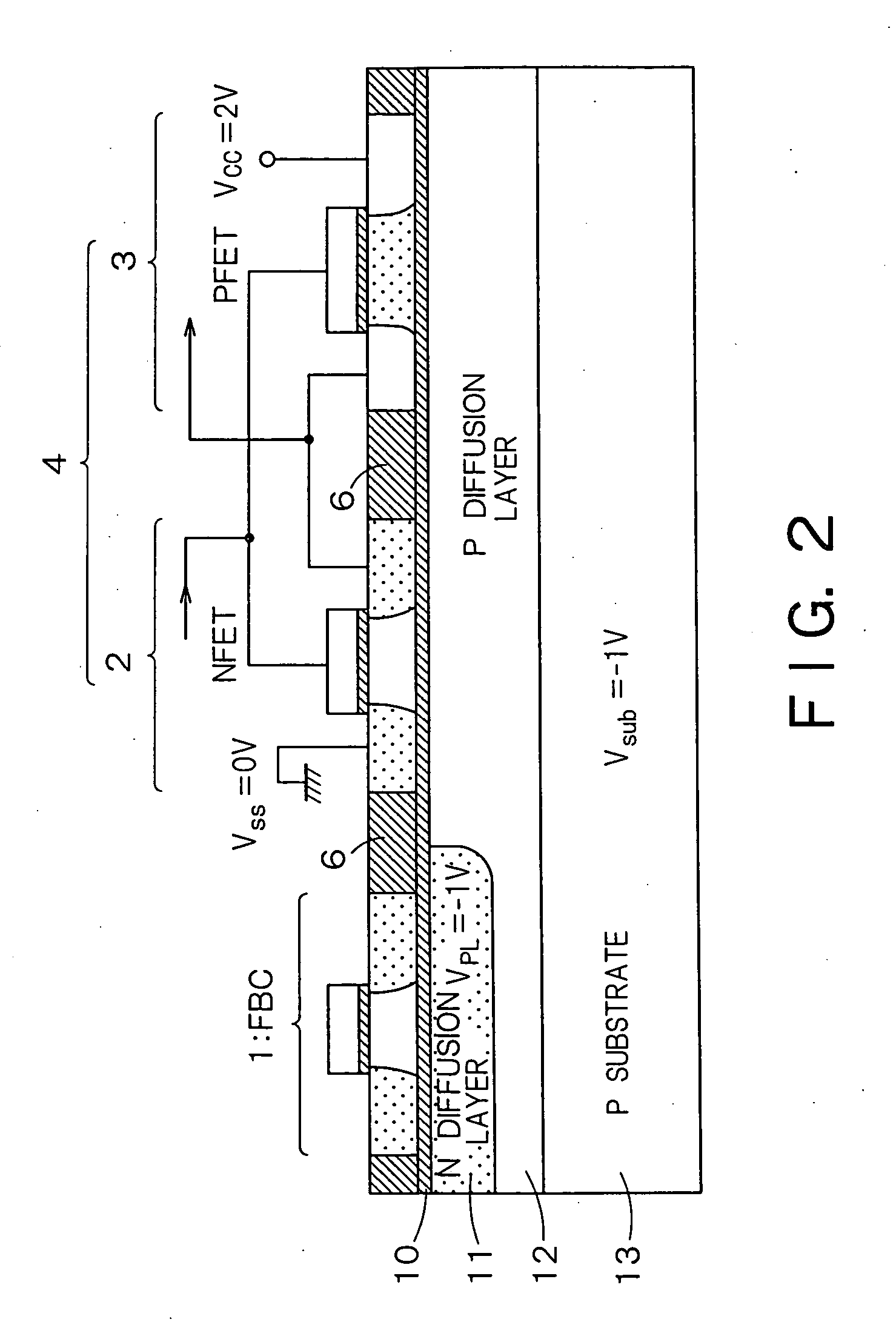
[0119] According to a second embodiment, different from the first embodiment, the plate potentials of the FBC 1, NFET 2, and PFET 3 are applied by the P diffusion layer.

[0120]FIG. 26 is a cross section showing the second embodiment of the semiconductor storage device according to the invention. The semiconductor storage device of FIG. 26 has an N diffusion layer (N-type well) 31 formed on the whole face of the P-type wafer 13, and a plurality of P diffusion layers 32, 33, and 34 formed in the N diffusion layer 31 by being separated from each other. The P diffusion layers 32, 33, and 34 are provided in correspondence with the FBC 1, NFET 2, and PFET 3, respectively. To the P diffusion layers 32, 33, and 34, plate potentials are supplied.

[0121] Due to the influence of the difference (1V) between the work function of N-type silicon and the work function of P-type silicon, to provide the same transistor characteristics as those of FIG. 16, each of the potentials applied to the P diffu...

third embodiment

[0126] In a third embodiment, the plate potential of the FBC 1 is given by the P diffusion layer, and the plate potential of the NFET 2 and PFET 3 is given by the N diffusion layer.

[0127]FIG. 29 is a cross section view showing the third embodiment of the semiconductor storage device according to the invention. The semiconductor storage device has the P diffusion layer 41 formed on the whole top face of the P-type wafer 13, and N diffusion layers 42 and 43 which are formed on the P diffusion layer 41 by being separated from each other. The N diffusion layer 42 is formed below the NFET 2, and the N diffusion layer 43 is formed below the PFET 3. The same potential is applied to the P-type wafer 13 and the P diffusion layer 41.

[0128] By the influence of the difference of about 1V between the work function of the P type silicon and the work function of the N type silicon, in the case of FIG. 29, the potential higher than that in FIG. 16 by about 1V is applied to the P-type wafer 13, th...


PUM


Abstract

A semiconductor storage device according to the present invention, comprising: a first semiconductor layer formed on a substrate via a buried insulation layer; an FBC (Floating Body Cell) having a channel body of floating type formed on the first semiconductor layer, a main gate which forms a channel at a first face side of the channel body, and an auxiliary gate formed to capacitively couple on a second face at an opposite side of the first face; a logic circuit formed on the first semiconductor layer, separate from the FBC by an insulation film, which transfers a signal for the FBC; a second semiconductor layer which locates below the FBC and is formed along an under face of the buried insulation film; and a third semiconductor layer which locates below the logic circuit and is formed along an under face of the buried insulation film, wherein the second and third semiconductor layers are set to be in a potential different from each other.

Description

CROSS REFERENCE TO RELATED APPLICATIONS [0001] This application claims benefit of priority under 35USC§119 to Japanese Patent Application No. 2003-188413, filed on Jun. 30, 2003, the entire contents of which are incorporated by reference herein. BACKGROUND OF THE INVENTION [0002] 1. Field of the Invention [0003] The present invention relates to a semiconductor storage device and a semiconductor integrated circuit and, more particularly, to an FBC (Floating Body Cell) memory for storing information by accumulating majority carriers in a floating body of a field effect transistor (FET). [0004] 2. Related Art [0005] It is concerned that as a DRAM cell constructed by a conventional one transistor and one capacitor having a trench capacitor and a stacked capacitor is becoming smaller, it is becoming difficult to fabricate the DRAM cell. As a memory cell which can replace such a DRAM cell, a new memory cell, an FBC, for storing information by accumulating majority carriers in a floating c...

Claims


Application Information

Patent Timeline
Patent Type & Authority Applications(United States)
IPC IPC(8): H01L29/94H01L27/04G11C5/14G11C11/404G11C11/407G11C11/4074H01L21/82H01L21/822H01L21/8238H01L21/8242H01L27/08H01L27/088H01L27/092H01L27/10H01L27/108H01L27/12H01L29/786
CPCH01L27/1203H10B99/00H10B12/00
Inventor OHSAWA, TAKASHI
Owner KK TOSHIBA
Learn More