Contactless wafer level burn-in

a technology of contactless wafers and burnins, which is applied in the testing/measurement of individual semiconductor devices, semiconductor/solid-state devices, instruments, etc., can solve the problems of short circuit between conductors, manufacturing defects, and excessive thinness of the insulating oxide layer between two conductors in a particular region

Inactive Publication Date: 2006-06-22
SANDISK TECH LLC
View PDF10 Cites 45 Cited by
  • Summary
  • Abstract
  • Description
  • Claims
  • Application Information

AI Technical Summary

Benefits of technology

[0022] In a still further aspect, the invention is an apparatus for burn-in self testing of a device. The apparatus includes a test chamber, a transport mechanism in the test chamber, a temperature control apparatus in the test chamber; and an RF transponder in the chamber. The apparatus may further include a test controller coupled to at least the temperature control apparatus and the RF transponder.
[0023] In another aspect, the invention is a method for manufacturing a semiconductor device. The method includes the steps of fabricating a plurality of devices on a semiconductor wafer; performing burn-in self testing of each of the devices by coupling power and control signals to the wafer via an RF signal; testing the devices; and separating the devices from the wafer.
[0024] In another aspect, a non volatile memory system is provided. The system includes an array of storage elements and con

Problems solved by technology

Not all die on a particular semiconductor wafer are completely functional; some have manufacturing defects.
For example, an insulating oxide layer between two conductors may be excessively thin in a particular region.
Voltage and temperature stress will cause the particular region of excessively thin insulating oxide to break down, resulting in a short circuit between the two conductors which can be detected during electrical testing.
The failure rate of an MCM increases with the number of die on the MCM.
Typically functional gross failures occur within the first 48 hours of stress testing with elevated ambient temperature of 125° C. and voltage levels 10% above nominal operating values.
A drawback with prior art wafer level burn-in concerns mismatch between the coefficients of thermal expansion of the test apparatus and the wafer during burn-in, as well as the adverse effects of a defective test app

Method used


Image

  • Contactless wafer level burn-in
  • Contactless wafer level burn-in
  • Contactless wafer level burn-in

Examples


Embodiment Construction

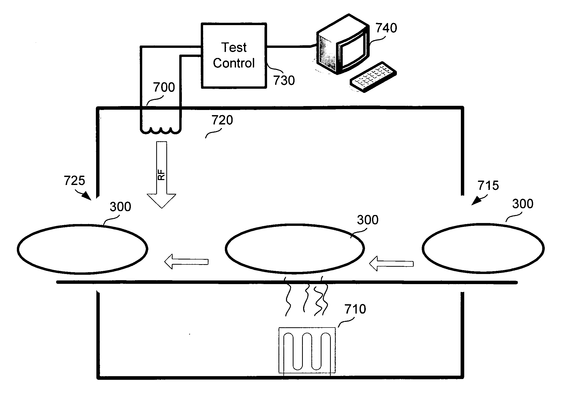
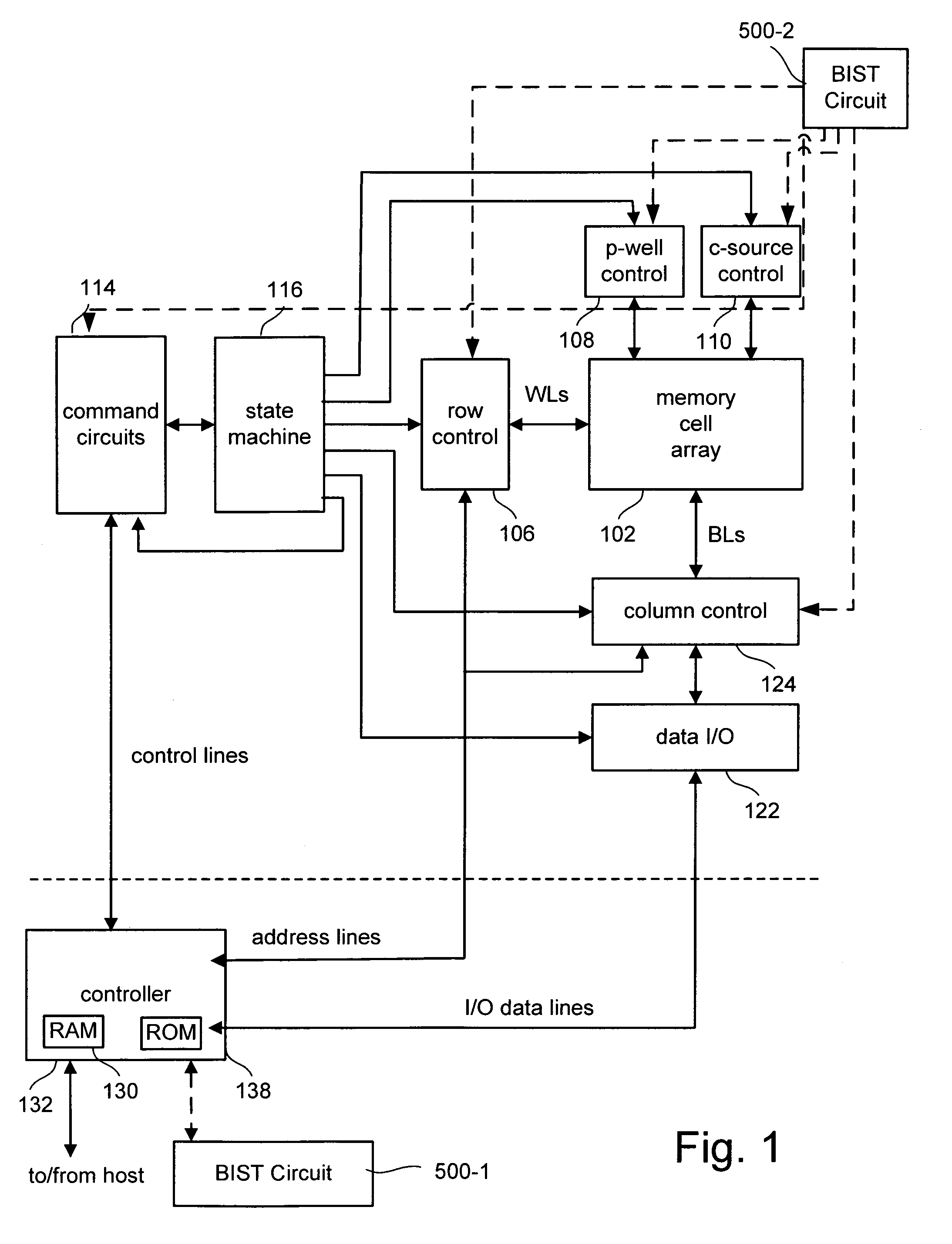
[0039] In accordance with the invention, a unique process for ensuring reliability in integrated circuits is provided. The invention provides a system and method for performing tests on a circuit die using an RF signal to deliver control and power to an on-wafer built-in self test (BIST) circuit. One example of a test which may be performed is a burn-in test, described herein. However, it will be understood additional types of tests may be performed using the method of the present invention. The circuit may be provided in the die or an alternative part of the wafer. An on-wafer RF antenna serves as the inductive secondary coil of the RF system which delivers power and instructions to the BIST circuit. Multiple BIST circuits may be provided, with an antenna associated with each circuit. In a further aspect, the antenna may be provided in metal layers in scribe lines separating the various die.

[0040] The invention has applications in various integrated circuit technologies, including...


PUM


Abstract

A method and apparatus for performing a wafer-level burn-in. The method comprises the steps of providing the wafer into a burn-in chamber; and outputting a power and a test initiation signal to a wafer via a wireless signal. The apparatus includes a test chamber, a transport mechanism in the test chamber, a temperature control apparatus in the test chamber, and an RF transponder in the chamber.

Description

BACKGROUND OF THE INVENTION [0001] 1. Field of the Invention [0002] The present invention is directed to apparatus and methods for ensuring reliability in semiconductor devices, and particularly for providing wafer level burn-in. [0003] 2. Description of the Related Art [0004] Semiconductor wafers typically comprise a plurality of substantially isolated “die” or “chips” containing circuitry, separated from each other by scribe line areas. In the normal integrated circuit production flow, an integrated wafer that has completed fabrication is cut into many individual die. The individual die contained within the wafer are separated by sawing and packaged individually or in multi-chip modules. These die are then mounted into individual sockets that can then be burned-in and tested using standard test equipment and fixtures. [0005] The demand for smaller and smaller consumer devices, such as wireless telephones and PDAs, has led to smaller semiconductor device packages and even to the us...

Claims


Application Information

Patent Timeline
IPC IPC(8): G01R31/26
CPCG01R31/2831G01R31/2856G01R31/2862G01R31/2884G01R31/3025G11C16/04G11C29/006G11C29/06G11C2029/1206G11C2029/5602G01R31/26G01R31/302H01L22/00
Inventor CHEN, JIAN
Owner SANDISK TECH LLC
Why Eureka
Try Eureka