
Semiconductor device and a method of manufacturing the same

a semiconductor device and semiconductor technology, applied in semiconductor devices, digital storage, instruments, etc., can solve problems such as product operation troubles and disturbances, and achieve the effect of improving the reliability of the semiconductor device having a nonvolatile memory element and reducing the size of the semiconductor devi

Inactive Publication Date: 2006-06-22
RENESAS TECH CORP
View PDF6 Cites 17 Cited by
  • Summary
  • Abstract
  • Description
  • Claims
  • Application Information

AI Technical Summary

Benefits of technology

[0010] In view of the above, we contemplate to provide a structure wherein the position of occurrence of hot holes is kept apart from the gate electrode so that the hot holes becomes unlikely to suffer the influence of the gate bias and surface potential, and thus the injection efficiency of the charge retention layer is reduced, thereby suppressing the occurrence of the disturb. The invention has been accomplished based on this.
[0011] It is accordingly an object of the invention to provide a technique related to a semiconductor device having a nonvolatile memory element, in which the efficiency of injection of hot holes occurring by application of stress into a charge storage layer can be reduced.
[0012] It is another object of the invention to provide a technique capable of improving reliability of a semiconductor device having a nonvolatile memory element.
[0035] According to the invention, reliability of the semiconductor device having a nonvolatile memory element can be improved.

Problems solved by technology

We made studies on a semiconductor device having a MONOS nonvolatile memory element and, as a result, found the following problems involved therein.
In a nonvolatile MONOS memory mounted in IC cards, when a negative high voltage stress is continuedly exerted on a gate electrode and a substrate (well region) through bits (memory cells) wherein electrons have been injected into a charge retention layer (i.e. an insulating film (ONO film) for charge storage), a disturb mode wherein a threshold voltage lowers takes place, with a possibility that troubles arise in product operation.
This disturb mode involved in the stress occurs such that the potential difference between a diffusion layer and a substrate (or a gate electrode) is so great that hot holes are produced at the pn junction of the diffusion layer and the substrate, and these holes are injected into the charge retention layer, thereby causing the disturb to occur.

Method used


Image

  • Semiconductor device and a method of manufacturing the same
  • Semiconductor device and a method of manufacturing the same
  • Semiconductor device and a method of manufacturing the same

Examples


embodiment 1

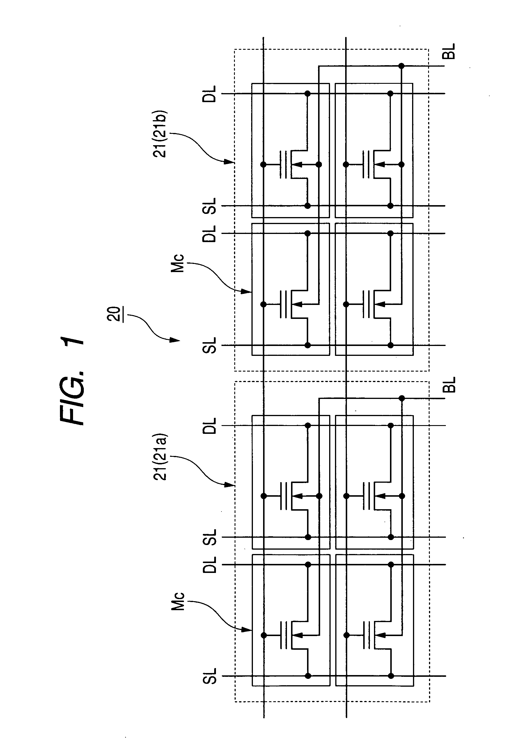
[0050] In Embodiment 1, an instance of application of the invention to a flush memory (semiconductor device) wherein a memory cell is constituted of a MONOS nonvolatile memory element.

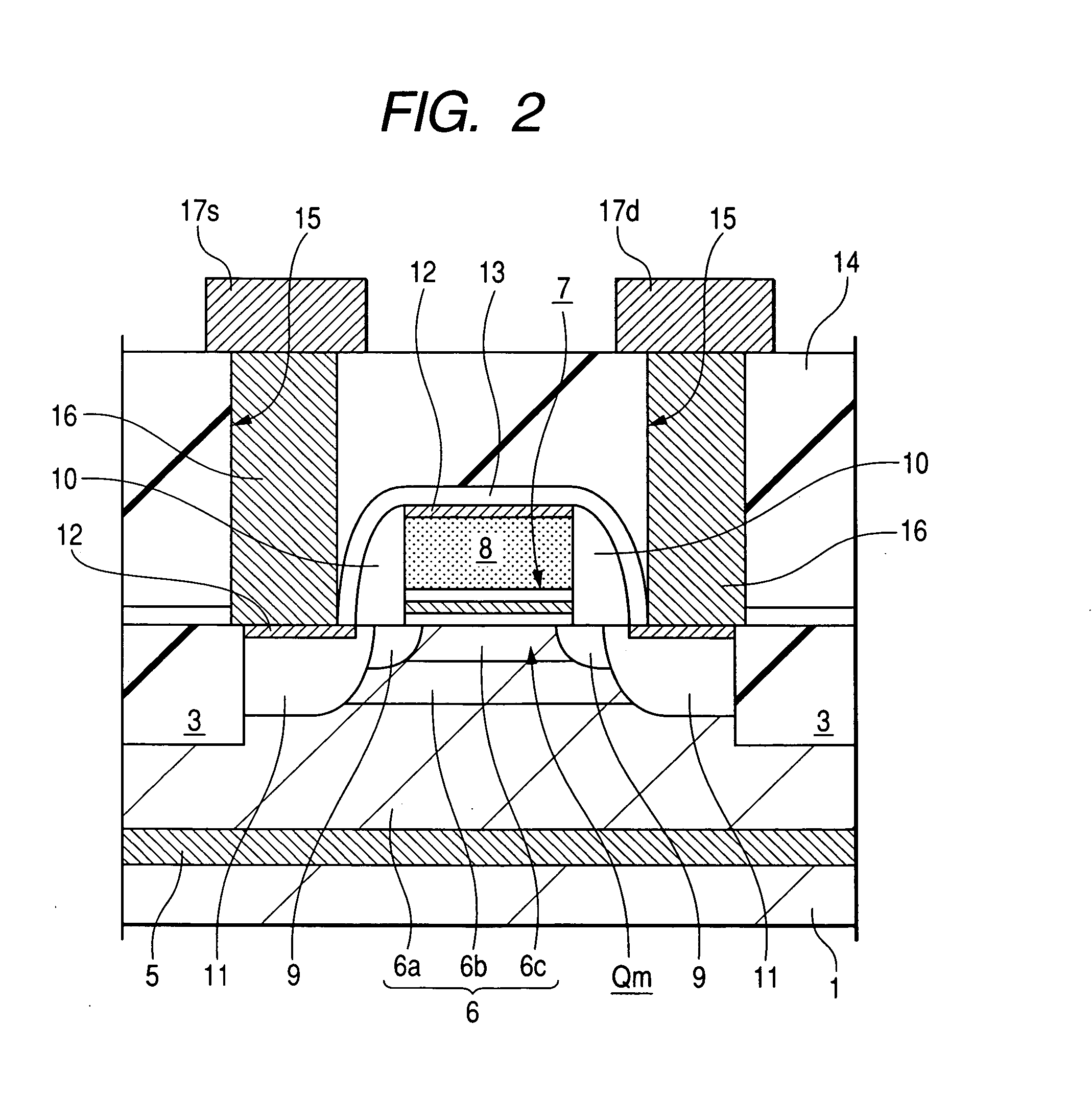
[0051] FIGS. 1 to 15 are views related to a flush memory according to Embodiment 1 of the invention, respectively.

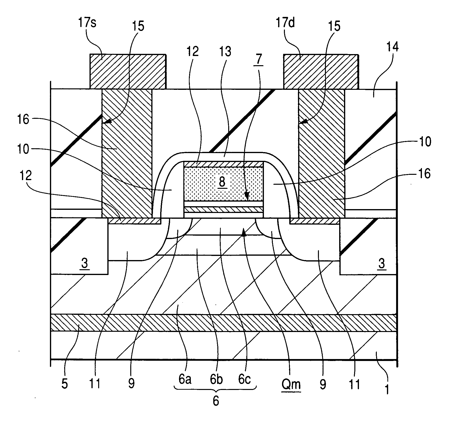
[0052] More particularly, FIG. 1 is an equivalent circuit diagram showing a memory array arrangement of the flush memory (semiconductor device), FIG. 2 is a schematic sectional view showing a schematic arrangement of nonvolatile memory elements mounted in the memory cell array, and FIG. 3 is a schematic, enlarged, sectional view of part of FIG. 2. FIGS. 4(a) and 4(b) are, respectively, an impurity concentration distribution wherein FIG. 4(a) is a graph showing an impurity concentration distribution along line a-a of FIG. 3 and FIG. 4(b) is an impurity concentration distribution along line b-b of FIG. 3. FIGS. 5 to 15 are, respectively, a schematic sectional view showing a manufacturing st...

embodiment 2

[0117] In a nonvolatile MONOS memory mounted in current IC cards, there exists a mode wherein a threshold voltage increases, aside from the disturb mode illustrated in the above Embodiment 1, when a negative, high voltage stress is continuously exerted on a substrate against bits wherein holes have been injected into the charge retention layer. This mode results as follows: high voltage application to the substrate has a surface potential beneath the gate electrode increased, so that electrons are injected into the charge retention layer owing to the potential difference with the charge retention layer. Accordingly, in order to avoid the disturb mode produced through the increasing threshold voltage, it becomes necessary to lower the surface potential beneath the gate electrode, for which it is effective to make the well low in concentration. However, the low concentration of the well is in trade-off relation with the disturb mode occurring through the lowering of threshold voltage....


PUM


Abstract

A semiconductor device having a well region of a first conduction type formed in a main surface of a semiconductor substrate, and a nonvolatile memory element formed at the well region is provided. The nonvolatile memory element comprises a gate electrode formed over the well region through an insulating film for charge storage, and a source region and drain region of a second conduction type which are separated from each other and are disposed in the well region. The well region includes a third semiconductor region, a second semiconductor region which is arranged at a position deeper than the third semiconductor region, and a first semiconductor region that is arranged at a position deeper than the second semiconductor region. The first and third semiconductor regions, respectively, have an impurity concentration higher than the second semiconductor region.

Description

CROSS-REFERENCE TO RELATED APPLICATION [0001] The present application claims priority from Japanese patent application No. 2004-358083 filed on Dec. 10, 2004, the content of which is hereby incorporated by reference into this application. BACKGROUND OF THE INVENTION [0002] This invention relates to a semiconductor device and a manufacturing technique therefor. More particularly, the invention relates to a technique effective for application to a semiconductor device having a nonvolatile memory element. [0003] For a semiconductor device, a nonvolatile semiconductor memory device called, for example, a flush memory is known. In the memory cells of this flush memory, there are known a one-transistor system constituted of one nonvolatile element, and a two-transistor type wherein one nonvolatile memory element and one MISFET (metal insulator semiconductor field effect transistor) for selection are connected in series. The nonvolatile memory elements known in the art are those of a float...

Claims


Application Information

Patent Timeline
Patent Type & Authority Applications(United States)
IPC IPC(8): G11C16/04
CPCG11C16/0416G11C16/3418G11C16/3427H01L29/66833H01L29/792
Inventor MAEKAWA, KEIICHIMINAMI, SHINICHIWATANABE, KOZOKAMOHARA, SHIROYOSHIDA, SHOJI
Owner RENESAS TECH CORP
Learn More