Fabrication of array pH sensitive EGFET and its readout circuit

Inactive Publication Date: 2006-07-06
CHUNG YUAN CHRISTIAN UNIVERSITY
2 Cites 20 Cited by

AI-Extracted Technical Summary

Problems solved by technology

However, due to the relatively large volume, high cost and long reaction time, the technologies for fabricating these ion selective glass electrodes have been developed toward the technologies of established silicon semiconductor integrated cir...

Benefits of technology

[0032] An object of the invention is to provide a method for fabricating an array pH sensor and a readout circuit of such array pH sensor, wherein this fabrication method has a lot of advantages such as simple fabrication equipment, cost effectiveness, mass production, etc. so as to be suitable for fabricating disposable sensors. Therefore, in the field of the array pH sensor, the present invention is highly feasible and applicable.
[0033] The method for fabricating an array pH sensor and a ...

Abstract

A method for fabricating an array pH sensor and a readout circuit device of such array pH sensor are implemented by utilizing an extended ion sensitive field effect transistor to construct the array pH sensor and related readout circuit. The structure of the array sensor having this extended ion sensitive field effect transistor comprises a tin dioxide/metal/silicon dioxide multi-layer structure sensor and a tin dioxide/indium tin oxide/glass multi-layer structure sensor and has excellent properties. Furthermore, the readout circuit and the sensor utilize two signal generators for controlling and reading signals. In particular, the sensor can be effective for increasing the accuracy of measurement and reducing the interference of noise.

Application Domain

Technology Topic

PhysicsIon sensitive +5

Image

  • Fabrication of array pH sensitive EGFET and its readout circuit
  • Fabrication of array pH sensitive EGFET and its readout circuit
  • Fabrication of array pH sensitive EGFET and its readout circuit

Examples

  • Experimental program(1)

Example

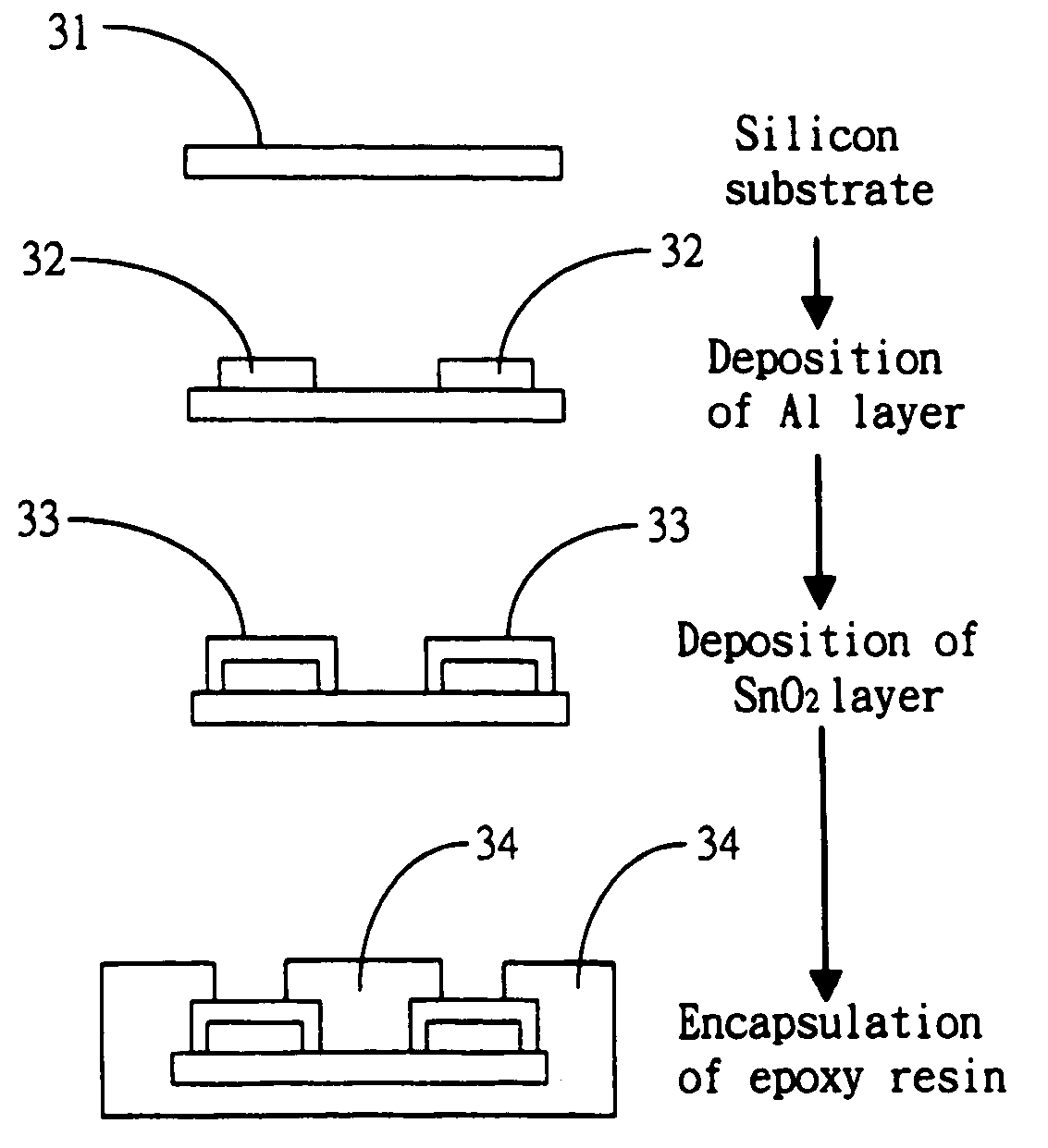
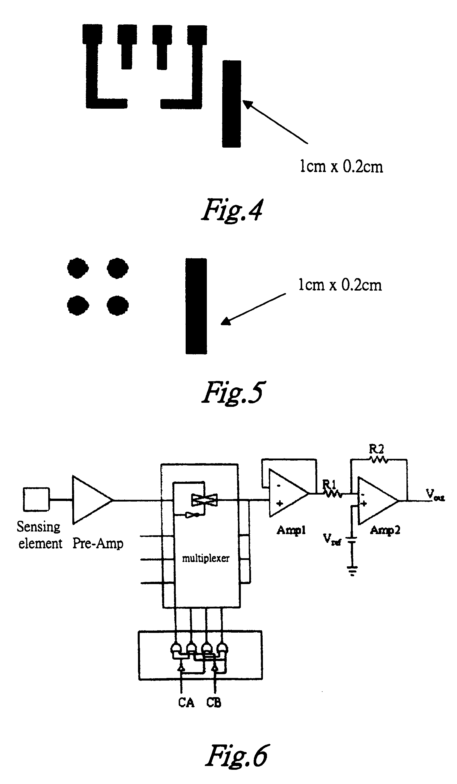
[0050] The method for fabricating an array pH sensor and its readout circuit of the present invention are implemented by depositing a non-conductive pH sensing film onto a non-insulated substrate, thereby fabricating a separate array pH sensor and detecting the pH value of the solution by using such array pH sensor. In addition, the readout circuit of this array pH sensor, which includes pre-readout circuit, a multiplexer, a rear end buffer circuit and an amplifier circuit, is fabricated according to the typical processes for making semiconductors. The array pH sensor and the readout circuit can be combined to be a hybrid array pH sensor. The array sensor is advantageous over the single sensing element, because larger sampling signals can decrease error resulting from the sensing element and accuracy thereof is increased. When it is commercialized, the sensor would have high stability and accuracy.
[0051] The metal oxide thin-films were prepared by the radio frequency sputtering system (SnO2 target: 99.9%) at a substrate temperature of 150° C. The sensing part of the sensor was based on the SnO2 thin film and the SnO2 thin film was deposited onto the ITO glass by the radio frequency sputtering method. Before depositing the SnO2 thin film, the ITO glasses were washed by methyl alcohol and deionized (D.I.) water. Finally, the device was bounded and packaged to form the SnO2 pH electrode by epoxy.
[0052] The extended ISFET can be fabricated when the sensing devices and readout circuits are separated. Additionally, based on the previous reports, several types of sensors were fabricated based on a separated structure, including the pH sensor [3, 4], the acetyicholine sensor [5], the glucose sensor [6] and the pH-sensitive electrode-based urea sensor [7].
[0053] As mentioned above, the extended-gate field effect transistor was separated into two parts; one was a sensing structure containing the sensitive membrane and another was a MOSFET structure. Therefore, the circuit part (MOSFET structure) of the sensing structure could be reused and the sensitive membrane part is served as a deposable device. That is to say, the cost of the extended-gate field effect transistor is lower than the ion sensitive field effect transistors.
[0054] The process for fabricating the array sensor of the present invention comprises the following steps:
[0055] Step 1: providing a p-type silicon substrate with resistivity of 4˜7 Ohm-cm and silicon dioxide of 1000 angstrom;
[0056] Step 2: growing an Al film by using a metallic mask and a vacuum evaporation machine;
[0057] Step 3: growing a SnO2 film by using a metallic mask and a sputter machine; and
[0058] Step 4: encapsulating the resulting product with epoxy resin.
[0059] The readout circuit portion is fabricated according to a 0.5 micrometer 2P2M n-well process provided by United Microelectronics Corp. (Hsinchu, TW), wherein the related processing conditions are shown in FIG. 14. The features for each layer of the sensor can be illustrated as follows:
[0060] 1. The thickness of Cpoly is 0.2 micrometer (μm);
[0061] 2. The thickness of Gpoly is 0.3 micrometer (μm);
[0062] 3. The thickness of Metal 1 is 0.6 micrometer (μm);
[0063] 4. The thickness of Metal 2 is 1.1 micrometer (μm);
[0064] 5. The thickness of Passivation layer is 0.7 micrometer (μm);
[0065] 6. The thickness of gate oxide layer is 135 angstrom (Å); and
[0066] 7. The total area of the chip is 1.8 mm2.
[0067]FIG. 1 is the cross-sectional view showing a sensing configuration of SnO2/Al/SiO2/Si. As can be seen in FIG. 1, such structure is easily fabricated according to the standard CMOS fabrication process, and can be a tin dioxide/aluminum metal/silicon dioxide structure 1, which is constructed by depositing an aluminum layer 12 and a tin dioxide layer 13 onto a substrate 11, and encapsulating the resulting structure with epoxy resin 14 to form a opening channel. Via the aluminum layer 12, a conducting line 4 is led out.
[0068]FIG. 2 is the cross-sectional view showing the sensing configuration of SnO2/ITO/glass. Since the glass substrate is cost effective, the sensor with this structure can be applied to fabricate disposable sensors. This structure is a tin dioxide/indium tin oxide/glass structure 2, which is constructed by depositing an indium tin oxide layer 22 and a tin dioxide layer 23 onto a glass substrate 21, and partially encapsulating the resulting structure with epoxy resin 24 to form a opening channel. Via the indium tin oxide layer 22, a conducting line 4 is led out.
[0069] Please refer to FIG. 3. The flowchart for fabricating the array pH sensor of the present invention comprises the following steps:
[0070] Step 1: providing a silicon substrate 31, for example a p-type silicon substrate with resistivity of 4˜7 Ohm-cm and silicon dioxide layer of 1000 angstrom, wherein the silicon substrate can be replaced by glass substrates, ceramic substrates or polymeric substrates in order to broaden the applications of the sensor;
[0071] Step 2: growing an Al film 32 by using a metallic mask and a vacuum evaporation machine;
[0072] Step 3: growing a SnO2 film 33 by using a metallic mask and a sputter machine; and
[0073] Step 4: encapsulating the resulting product with epoxy resin 34.
[0074] The process for fabricating such sensor is easy because the procedures of coating photoresist solutions and etching films are omitted.
[0075]FIG. 4 is a schematic view showing the Al layer mask, which is a metallic mask. The portions of the aluminum film to be deposited are indicated with the black portions. After the metallic mask is etched away, the Al film is deposited onto the metallic portions where the mask has been removed.
[0076]FIG. 5 is a schematic view showing the sensing membrane SnO2 layer mask, which is a metallic SnO2 mask. The portions of the tin dioxide film to be deposited are indicated with the black portions. After the metallic mask is etched away, the tin dioxide film is deposited onto the metallic portions where the mask has been removed.
[0077]FIG. 6 is the configuration of the array pH sensor of the present invention. This array pH sensor comprises four sensing elements and four pre-amplifiers at the front end thereof. The respective sensing element is read by control circuits, and the pre-amplifier and the control circuits are compensated by the rear end amplifiers, thereby obtaining an output/input ratio of 1. The rear end readout circuit of this array sensor can be used to receive different signals and amplifying these signals for determination. Thus, when the multiplexer is modified, a variety of array sensors can be fabricated for many applications such as fabrication of potentiometric sensor.
[0078]FIG. 7 is the circuit configuration of the pre-amplifier for the array pH sensor. The pre-amplifier is consisted of four CMOS devices so as to reduce the layout space.
[0079]FIG. 8 shows the input/output ratio of the pre-amplifier. The output/input ratio is 0.7184 and an offset voltage is −1.097V. Accordingly, the signal would be decreased, when the sensing element is connected to the pre-amplifier.
[0080]FIG. 9 shows the circuit configuration of the switch of the control portion, which is consisted of an inverter and a CMOS switch.
[0081]FIG. 10 shows the circuit configuration of a 2 to 4 decoder of the control portion, which is consisted of six inverters and four NAND circuits.
[0082]FIG. 11 is a schematic diagram showing the output/input ratio of the circuit combined the pre-amplifier and the control circuit. The output/input ratio is 0.675 and the offset voltage is −1.095V. Accordingly, the signal would be further decreased, when the sensing element was connected to the pre-amplifier and multiplexer.
[0083]FIG. 12 is a schematic diagram showing the output/input ratio of the circuit of the array pH sensor. As can be seen in FIG. 12, due to the amplification of the rear end readout circuit, the signals of the sensing membrane can be compensated to the initial values and the ratio of the output voltage to the input voltage is 1.04.
[0084] It was in order to compensate the decreasing of pre-circuit. So, The input output ratio is 1.04 of the array pH sensor system, when the circuit included the pre-amplifier, multiplexer, buffer and post amplifier.
[0085]FIG. 13 is a schematic diagram showing the readout signal of the array pH sensor. As can be seen in FIG. 13, four sets of signals are stable, indicating a stable fabrication process of this array sensor.
[0086]FIG. 14 is a schematic correction curve of the readout signal of the array pH sensor. The correction curve shows a linear pH sensitivity of 0.99969, which indicates an excellent performance of the array ion sensor.
[0087]FIG. 15 is a cross-section view showing the related processes for fabricating a chip. In FIG. 15, the relative positions of the layer structures of a 0.5 micrometer n-well double polysilicon double-metal process are shown.
[0088] Many changes and modifications in the above described embodiment of the invention can, of course, be carried out without departing from the scope thereof. Accordingly, to promote the progress in science and the useful arts, the invention is disclosed and is intended to be limited only by the scope of the appended claims.

PUM

no PUM

Description & Claims & Application Information

We can also present the details of the Description, Claims and Application information to help users get a comprehensive understanding of the technical details of the patent, such as background art, summary of invention, brief description of drawings, description of embodiments, and other original content. On the other hand, users can also determine the specific scope of protection of the technology through the list of claims; as well as understand the changes in the life cycle of the technology with the presentation of the patent timeline. Login to view more.

Similar technology patents

Wave filter for rotary filter

InactiveUS20020074278A1Cost effectivenessEasily removableFrozen sweetsConfectioneryPolymer meltWave shape
Owner:ALTER INVEST FUND LP

Radiation tube structure

Owner:WANG CHIUNG CHUAN

Plants with altered cell wall biosynthesis and methods of use

InactiveUS20130102022A1Easily releaseCost effectivenessCellulosic pulp after-treatmentBiofuelsCell wall biosynthesisPhenotype
Owner:UNIV OF GEORGIA RES FOUND INC

Classification and recommendation of technical efficacy words

  • Cost effectiveness

Wave filter for rotary filter

InactiveUS20020074278A1Cost effectivenessEasily removableFrozen sweetsConfectioneryPolymer meltWave shape
Owner:ALTER INVEST FUND LP

Radiation tube structure

Owner:WANG CHIUNG CHUAN
Why Eureka
Try Eureka