Solar cell and semiconductor device, and manufacturing method thereof

a technology of solar cells and semiconductors, applied in sustainable manufacturing/processing, instruments, horology, etc., can solve problems such as easy cracks, and achieve the effect of improving throughput and reducing the size and weight of solar cells

Inactive Publication Date: 2006-07-20
SEMICON ENERGY LAB CO LTD
View PDF37 Cites 33 Cited by
  • Summary
  • Abstract
  • Description
  • Claims
  • Application Information

AI Technical Summary

Benefits of technology

[0015] According to the present invention, miniaturization of an electrode layer and an insulating isolation layer can be realized. Accordingly, the number of cells per unit area can be increased to improve throughput. Further, since a contact angle between a photoelectric conversio

Problems solved by technology

Especially, a solar cell using an organic resin material for the substrate is thin and lightweigh

Method used


Image

  • Solar cell and semiconductor device, and manufacturing method thereof
  • Solar cell and semiconductor device, and manufacturing method thereof
  • Solar cell and semiconductor device, and manufacturing method thereof

Examples


embodiment 1

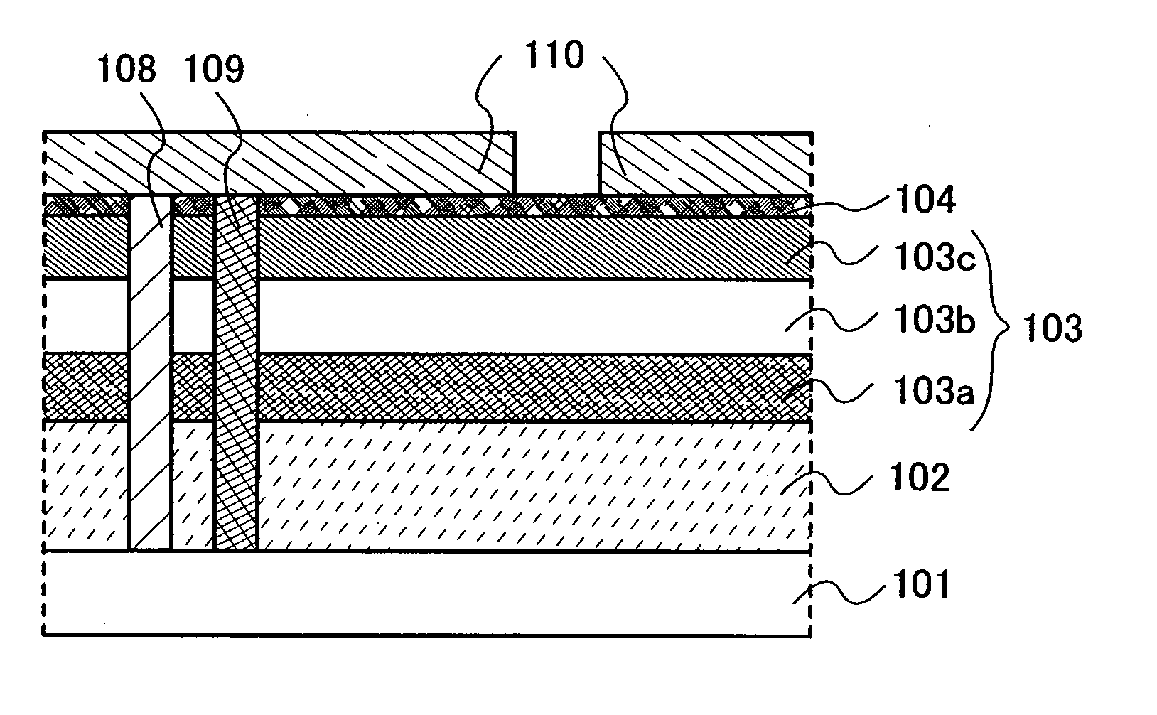
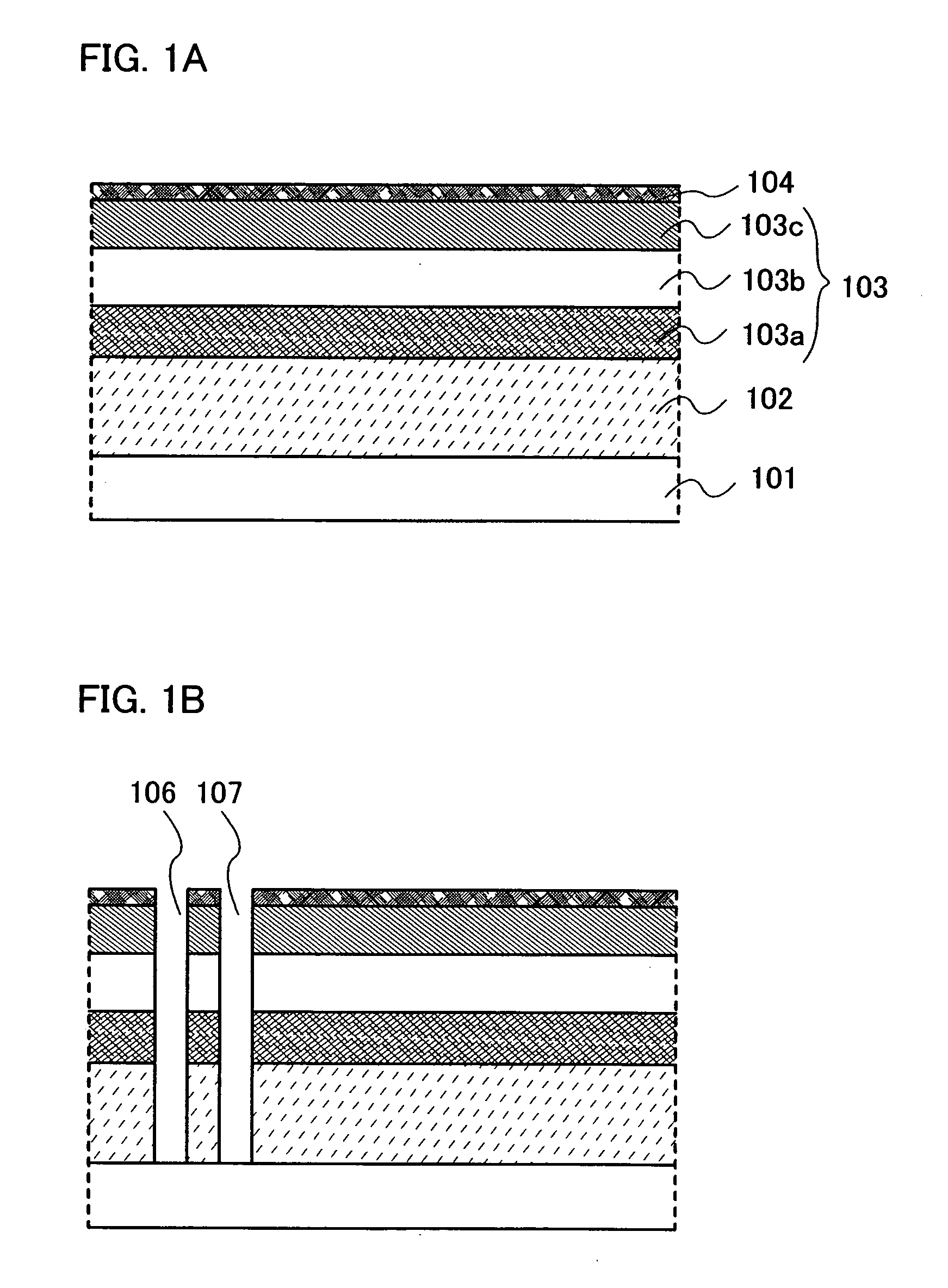
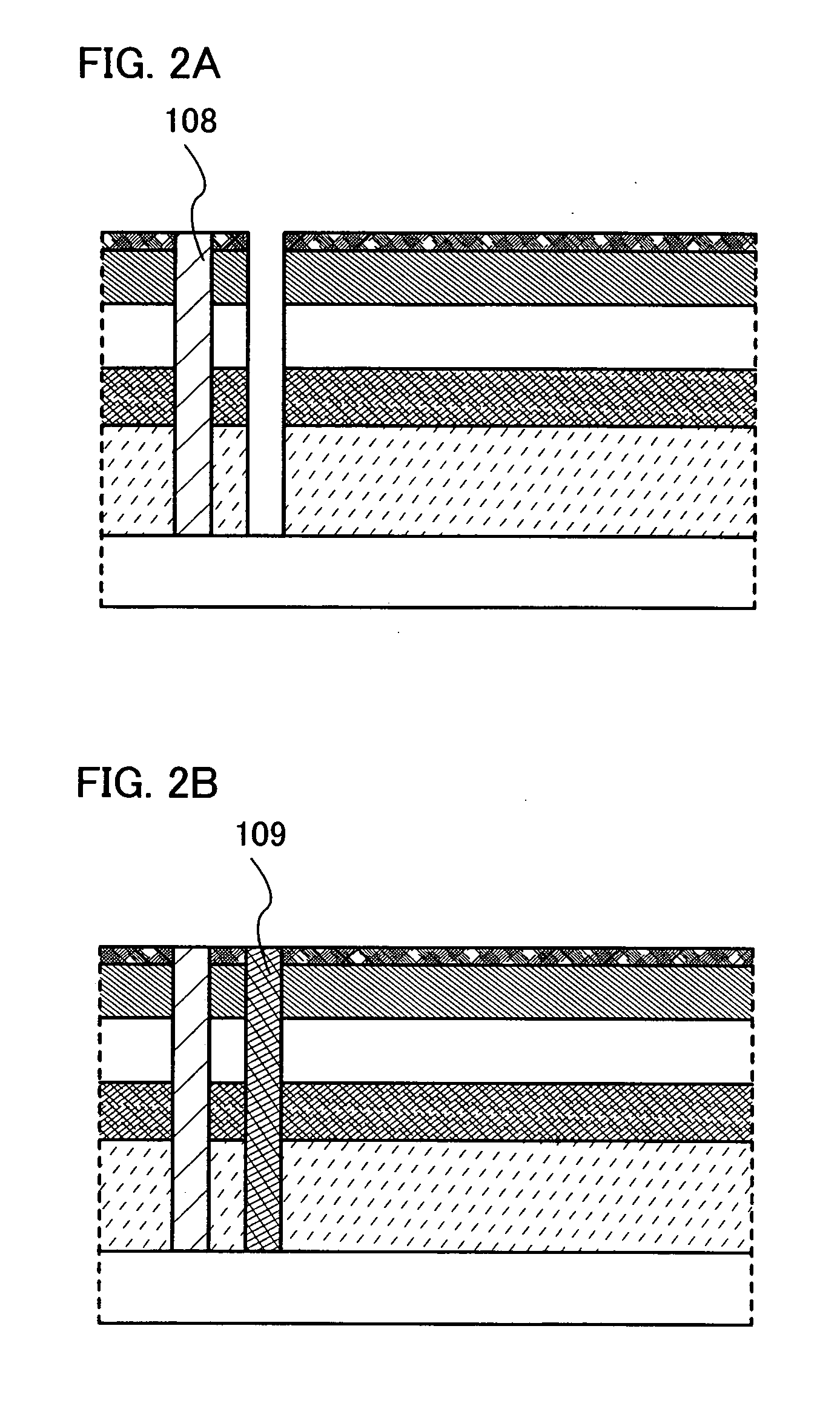
[0046] This embodiment is described with reference to FIGS. 4A to 4C, 5, and 6. In this embodiment, a method for manufacturing an integrated solar cell in which an organic resin material is used for a substrate and a plurality of unit cells is connected in series on one substrate is described.

[0047] In FIG. 4A, a translucent organic resin material such as polyethylene terephthalate (PET), polyethylene naphthalate (PEN), or polyethersulfone (PES) is used for a substrate 501. Of course, commercially available soda-lime glass, alkali-free glass, or a stainless substrate can also be used.

[0048] A sheet-like substrate of a suitable size may be used as the substrate 501. When manufacturing a solar cell according to this embodiment by a roll-to-roll method, a rolled substrate may be used. In the case where a roll-to-roll method is applied, an organic resin film substrate having a thickness of 60 to 100 μm is preferably used.

[0049] The solar cell manufactured in this embodiment has such ...

embodiment 2

[0081] In this embodiment, examples of various electrical devices having a solar cell manufactured according to the present invention are described with reference to FIGS. 7, 8A to 8C, and 9.

[0082]FIG. 7 is a top view of a solar cell according to this embodiment seen from a rear electrode side. FIG. 7 shows an example of a wrist watch in which a solar cell placed at the lower side (portion in which a movement of a wrist watch is installed) of a semitranslucent dial. A substrate 601 is an organic resin film having a thickness of 70 μm. Although any of the organic resin materials referred in Embodiment 1 can be applied, a PEN substrate is typically used for the substrate 601. The shape of the substrate 601 is not limited to a circle. An insertion port 607 of a pointer shaft is provided at the center.

[0083] In the solar cell, a transparent electrode layer, a photoelectric conversion layer, a rear electrode layer, and a sealing resin layer are stacked over the substrate 601 sequential...


PUM


Abstract

It is an object of the present invention to minimize an electrode in a solar cell to minimize the solar cell. The present invention provides a method for manufacturing a solar cell comprising the steps of forming a first electrode layer over a substrate, forming a photoelectric conversion layer over the first electrode layer, forming an organic layer over the photoelectric conversion layer, forming an opening reaching the first electrode layer in the photoelectric conversion layer, and forming a second electrode layer by filling the opening with a conductive paste, wherein the organic layer modifies the surface of the photoelectric conversion layer and a contact angle between the conductive paste and the photoelectric conversion becomes greater. According to the present invention, wettability of a photoelectric conversion layer can be decreased by forming an organic layer on a surface of the photoelectric conversion layer. Thereby an electrode layer and an insulating isolation layer can be thinned.

Description

BACKGROUND OF THE INVENTION [0001] 1. Field of the Invention [0002] The present invention relates to a structure of a semiconductor device such as a solar cell and a manufacturing method thereof [0003] 2. Description of the Related Art [0004] A solar cell has been spread not only to be used as a solar electric power generation system installed outdoors but also to be used as a power source of an electronic device with low power consumption such as a calculator, a radio, and a watch. In such a consumer use, when an appearance of an electronic device is as important as a function thereof as is the case for a wrist watch, for example, a mounting method of the solar cell is also devised. The solar cell is directly used as a dial of a watch, or is placed under a semitranslucent dial of the watch to make it unnoticeable. [0005] A large part of a solar cell is composed of a substrate formed from glass, stainless, or an organic resin material or the like, and a photoelectric conversion laye...

Claims


Application Information

Patent Timeline
IPC IPC(8): H01L31/00
CPCG04C10/02H01L31/022425H01L31/022466Y02E10/50H01L31/18H01L31/1884H01L31/202H01L31/048H01L31/022475H01L31/0465Y02P70/50E06B3/2605E06B2003/2625
Inventor NISHI, KAZUOAOKI, TOMOYUKIISA, TOSHIYUKIFUJII, GEN
Owner SEMICON ENERGY LAB CO LTD
Why Eureka
Try Eureka