Narrow linewidth semiconductor laser device

a semiconductor laser and narrow linewidth technology, applied in lasers, laser details, electrical equipment, etc., can solve the problems of large linewidth (5 khz), bulky, and relatively inefficient power consumption, and achieve high reliability

Active Publication Date: 2006-07-20
TERAXION
View PDF8 Cites 36 Cited by
  • Summary
  • Abstract
  • Description
  • Claims
  • Application Information

AI Technical Summary

Benefits of technology

[0027] Advantageously, the narrow linewidth semiconductor laser device of the present invention allows to provide an improved sub kHz linewidth while being compact, lightweight and highly reliable.
[0028] Moreover, the narrow linewidth semiconductor laser device o

Problems solved by technology

For applications where a large number of narrow linewidth lasers are required, cost is also a major issue.
In some of their realizations, they offer relatively high power and narrow linewidth (5 kHz) but are bulky and relatively power inefficient.
Single mode operation is also difficult to sustain without requiring the addition of special external controls like magnetic field, strain, temperature and so on.
One drawback is that they require specialty fibers with gratings, which can be expansive to produce and may not be well suited for some space application due to radiation sensitivity.
Another drawback comes from their sensitivity to environmental perturbations like vibrations, acoustic noise, strain or temperature.
Their linewidth, even if it is small, is not sufficient for applications where coherence length grater than 50 km is required.
These lasers are even more difficult to put under stable and reliable operation mode.
Since fiber lasers rely on a high power semiconductor laser to pump the active Erbium-doped fiber and do not use the output of the laser directly, these laser sources tend to be more complex, more costly, less reliable and less efficient than

Method used


Image

  • Narrow linewidth semiconductor laser device
  • Narrow linewidth semiconductor laser device
  • Narrow linewidth semiconductor laser device

Examples


Embodiment Construction

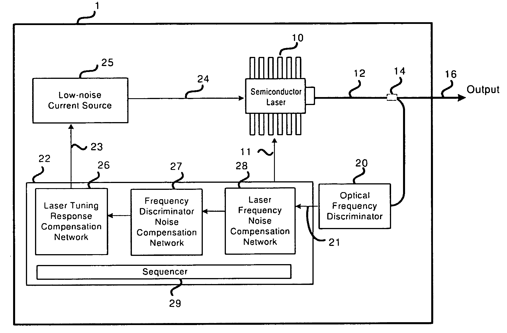
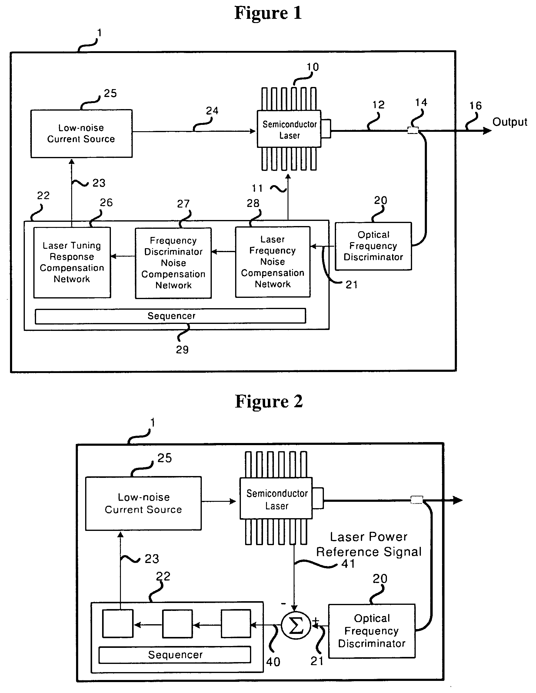
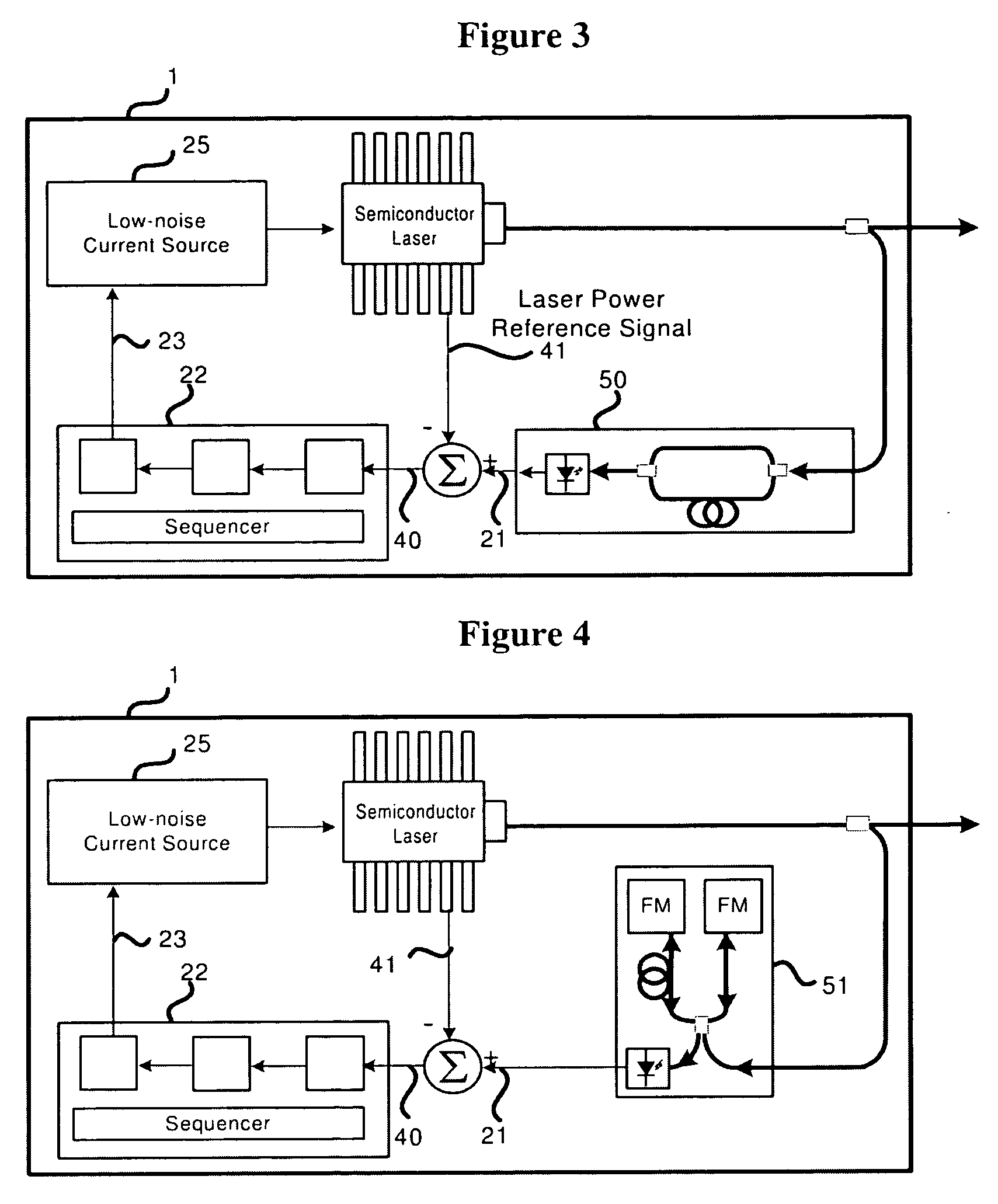
[0047] In the following description, similar features in the drawings have been given similar reference numerals and in order to lighten the figures, some elements are not referred to in some figures if they were already identified in a precedent figure.

[0048] The linewidth of semiconductor can be reduced by sending the laser light into a frequency discriminator that converts the frequency noise of the laser into intensity noise, by measuring this intensity with a photodetector and use this signal to compensate the frequency fluctuations of the laser by varying its injection current in an appropriate manner. Once the frequency locking loop thus described is established, the laser frequency will track very accurately the frequency fluctuations of the frequency discriminator within the bandwidth of that locking loop. The laser will therefore inherit the stability of the frequency discriminator. The short and medium term frequency noise of a well-designed frequency discriminator can b...


PUM


Abstract

There is provided a narrow linewidth semiconductor laser device comprising a semiconductor laser and a low noise current source operatively connected to the laser for supplying current thereto, the current source being particularly adapted to prevent a significant degradation of the frequency noise spectrum of the laser. The laser device also has an optical frequency discriminator providing an error signal representative of the optical frequency of the laser. The laser device also has control means having a feedback network for providing a frequency feedback signal. The feedback network is particularly adapted to the frequency noise spectrum of the frequency discriminator, the frequency noise spectrum of the laser and the tuning response of the laser. The control means is also provided with sequencing means for allowing to automatically enable frequency locking of the laser on the frequency reference of the optical frequency discriminator. The laser device is provided with an enclosure for enclosing the frequency discriminator to isolate the frequency discriminator from external perturbations. Such an arrangement is particularly advantageous since it allows to provide an improved sub-kHz linewidth and a high coherence while being compact, lightweight and highly reliable. Moreover, the narrow linewidth semiconductor laser device of the present invention can advantageously be automatically operated.

Description

FIELD OF THE INVENTION [0001] This invention generally relates to the field of high precision optical measurement and high resolution spectral analysis, and more particularly to the field of optical fiber sensing, laser radars (LIDARS), distance measurement, gas analysis, optical filter analysis, optical signal analysis and heterodyne detection. Thus, the present invention concerns a narrow linewidth semiconductor laser particularly adapted for these applications. BACKGROUND OF THE INVENTION [0002] Many applications require laser sources that offer a narrow linewidth, a high degree of coherence and low optical phase noise. [0003] Long baseline interferometry, for instance, rely on highly coherent lasers to detect extremely small length changes over tens and hundreds of kilometers by observing the change of phase of an optical beam after propagating through that distance. Gravitational wave detectors, formation-flying satellites and length-stabilized fiber distribution systems also u...

Claims


Application Information

Patent Timeline
IPC IPC(8): H01S3/10H01S3/13H01S3/00
CPCH01S5/042H01S5/0654H01S5/0687
Inventor CLICHE, JEAN-FRANCOISTETU, MICHELBARIBEAU, FRANCOISBLIN, STEPHANEGUY, MARTIN
Owner TERAXION
Why Eureka
Try Eureka