Method and apparatus for inspecting patterns

a pattern and pattern technology, applied in the field of inspection technology, can solve the problems of affecting the yield of semiconductor devices, affecting the accuracy of electron beam image magnification, and difficulty in optical image detection, etc., and achieves high efficiency, high accuracy, and optimal inspection conditions.

Inactive Publication Date: 2006-07-27
HITACHI HIGH-TECH CORP
View PDF11 Cites 15 Cited by
  • Summary
  • Abstract
  • Description
  • Claims
  • Application Information

AI Technical Summary

Benefits of technology

[0026] Further, from electron beam image information obtained when the potential of the electrode above the specimen is changed, a point of change with brightness of the electron beam image starting to decrease is selected as an inspecting condition, for display, or set as the inspecting condition. Further, the potential of the specimen or the potential of the electrode is extensively and coarsely changed in several stages, thereby obtaining the electron beam image in each of the stages. The point of change with the brightness of the obtained electron beam image starting to decrease is obtained from information on the obtained electron beam image. Then, the potential is changed in finer stages in the vicinity of the point of change, thereby obtaining the electron beam image in each of the finer stages again. Then, the point of change is obtained again from information on the electron beam image obtained again. An optimal inspecting condition can be thereby set with high efficiency and with high accuracy.
[0027] Assume the specimen (or substrate) such as the semiconductor device, having a fine circuit pattern formed thereon, or the wafer to be inspected in particular, of which the surface of the substrate is covered with an insulating film or which has the circuit pattern floated from the substrate. Then, using the technology described above, the potential of the substrate or the potential of the electrode for limiting charge, provided on the side of an electron beam source for irradiating the electron beam with respect to the substrate is determined so that a so-called state of equilibrium is maintained. In the state of equilibrium, the number of electrons pulled back from the substrate maintains equilibrium with the number of electrons returned to the substrate. Then, by setting this potential as the inspecting condition, the influence of charge on the specimen can be reduced.
[0028] According to the present invention, even for the wafer to be inspected that is easily subject to the influence of charge, it becomes possible to set the optimal inspecting condition for implementing stable inspection easily and with high accuracy. As a result, it becomes possible to perform highly sensitive inspection of a defect on the wiring test pattern which has been hitherto difficult to identify the location of the defect therein.
[0029] Further, when setting the optimal inspecting condition, conventionally, the defect detection sensitivity of the inspection and a set time for the inspection were varied according to the skill and the experience of an operator. On contrast therewith, according to the present invention, the optimal inspecting condition can be set in a short time. Accordingly, the time required for the operator to perform the inspection can be saved. A waiting period for products is also greatly reduced, so that a TAT (turnaround time) for detecting occurrence of a fault can be reduced. As described above, by providing the technology for inspecting the wiring step of the semiconductor device with high sensitivity and with high accuracy, the contents of a fault in the wiring step, which are important during the manufacturing process of the semiconductor device can be detected early. Further, information on the location and the size of the defect which is the cause of the fault necessary for taking countermeasures against the fault can be obtained substantially at the same time as the inspection. The TAT required until the countermeasures are taken can be thereby reduced, thus resulting in contribution to improvement in the yield and productivity of the semiconductor device.

Problems solved by technology

Whether the lithography process, etching process, and other various processes are satisfactory or not and generation of foreign matter during the manufacturing process of the semiconductor device greatly affect the yield of the semiconductor device.
With finer geometries of the circuit pattern, a more complicated shape of the circuit pattern, and diversification of materials, defect detection by the optical image has become difficult.
Such defects include an electric defect such as an open circuit or a short circuit in various transistors, and a conduction fault of an opening pattern.
Thus, a magnification for an electron beam image obtained during the inspection does not become accurate.
Hence, it has become difficult to continue the inspection with the same sensitivity and accuracy as those in the initial stage of the inspection.
It is therefore difficult to measure the charged potential real time based on the electron beam image alone.
However, when frequent suspension of the inspection and frequent focusing and positional alignment are performed on the wafer to be inspected, the time required for the inspection will become longer.
Hence, speeding up of the inspection has become difficult, which leads to an increase in the manufacturing cost of the semiconductor device.
An enormous time was therefore required for determining the optimal inspecting condition.
The quality of the electron beam image is not therefore stabilized.

Method used


Image

  • Method and apparatus for inspecting patterns
  • Method and apparatus for inspecting patterns
  • Method and apparatus for inspecting patterns

Examples


Embodiment Construction

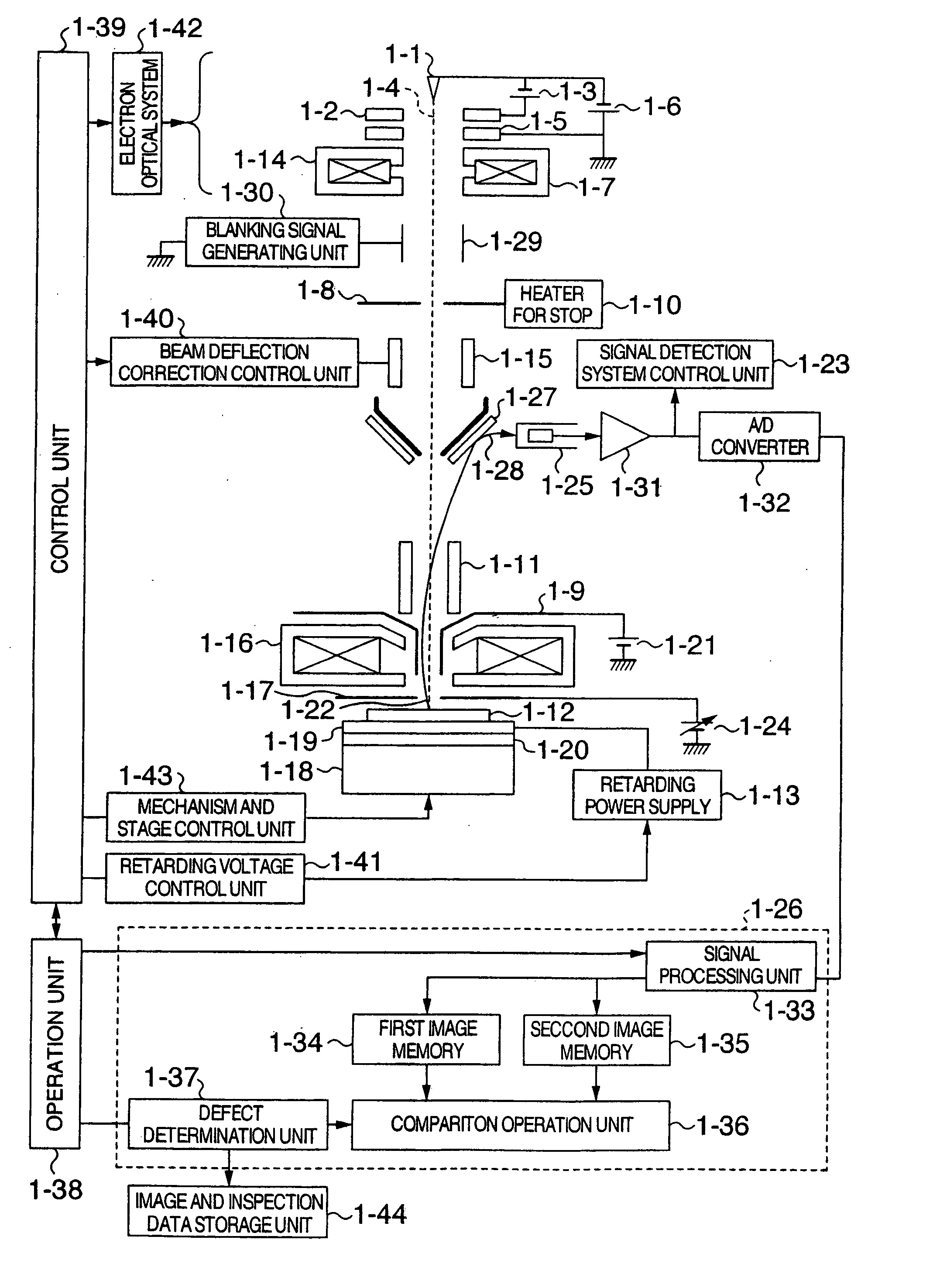
[0047] A technology of inspecting patterns according to an embodiment of the present invention will be described in detail with reference to drawings by taking inspection of a circuit pattern on a semiconductor device as an example.

[0048] First, before the embodiment of the present invention is described, the principle underlying the technology of inspecting the semiconductor device according to the present invention will be described in detail. The technology of inspecting presence or absence of a defect in a pattern such as the circuit pattern of the circuit having a structure floated from a substrate using an electron beam will be described, taking the circuit pattern of the semiconductor device formed on a wafer as an example.

[0049]FIG. 1 is a diagram showing an example of a configuration of an apparatus for inspecting the circuit pattern according to an embodiment of the present invention. The apparatus for inspecting the circuit pattern in this embodiment is roughly constitu...


PUM


Abstract

When the electrode potential of a charge control electrode above a wafer is reduced, image brightness is reduced. A point of change in the image brightness is a switching point between a positively charged state of the image and a negatively charged state of the image, showing the weakly charged state of the image. By setting this point of change as an inspecting condition, the amount of electric charges on the surface of the wafer can be reduced, and stable wafer inspection can be performed. It is estimated that an applied voltage V1 in FIG. 14 corresponds to the point of the change and is roughly included in the voltage range of a region enclosed by a broken line in the vicinity of the applied voltage V1. Within this voltage range, the influence of charge on an inspection under the inspecting condition can be reduced.

Description

CROSS-REFERENCE TO RELATED APPLICATION [0001] The present application is relevant to U.S. patent application Ser. No. ______ being filed by Yuko Sasaki, Yasuhiro Gunji and Chouki Tei, based on Japanese Patent Application No. 2004-367153 filed on Dec. 20, 2004, the entire content of which is incorporated herein by reference.BACKGROUND OF THE INVENTION [0002] The present invention relates to an inspection technology for inspecting fine patterns in a semiconductor device, a photo mask, a liquid crystal device, and the like. More specifically, the invention relates to the inspection technology for inspecting circuit patterns floated on a wafer during the manufacturing step of the semiconductor device, using an electron beam. [0003] The inspection technology for the semiconductor device, photo mask, and liquid crystal device having fine circuit patterns is a very important technology for improvement in a manufacturing yield thereof. An outline of the technology will be described below us...

Claims


Application Information

Patent Timeline
Patent Type & Authority Applications(United States)
IPC IPC(8): G21K7/00
CPCG01R31/307H01J37/026H01J37/04H01J37/263H01J37/28H01J2237/0048H01J2237/24592H01J2237/2817
Inventor NOZOE, MARIGOTO, YASUNORICHENG, ZHAOHUI
Owner HITACHI HIGH-TECH CORP
Why Eureka
Try Eureka