High performance MEMS packaging architecture

a packaging architecture and high-performance technology, applied in the field of micromachined sensor devices and methods, can solve the problems of limiting the level of performance achievable, mechanical die-stack, poor thermal conductivity, etc., and achieve the effect of reducing the effect of force applied, reducing the magnitude of force, and maximizing the utilization of common mode error cancellation

Inactive Publication Date: 2006-07-27
HONEYWELL INT INC
View PDF8 Cites 87 Cited by
  • Summary
  • Abstract
  • Description
  • Claims
  • Application Information

AI Technical Summary

Benefits of technology

[0019] The architecture of the die stack of the invention is limited to pure silicon, exclusive of the SiO2 isolator layers, which causes the die stack of the invention to be structurally very stiff, which in turn reduces effects of forces applied to the outside of the die-stack via the mounting flange.
[0020] The directional mounting flange and isolator between the die-stack and the user's mounting surface insulates the accelerometer proof mass from outside forces. Radial stress applied to the die-stack due to differential expansion between the silicon and the chassis material is a source of errors in MEMS devices, including MEMS accelerometer devices. Tines within the isolator portion of the directional mounting flange of the invention are compliant to radial expansion, but are stiff against in-plane and out-of-plane translation and rotatio

Problems solved by technology

However, architectures of current MEMS accelerometer and other devices limit the level of performance achievable.
Some limitations typical of prior art devices include the mechanical die-stack containing multiple different materials having different coefficients of thermal expansion, some with poor thermal conductivity.
This differential expansion also causes high residual stresses to be present in the different joined materials near the interface.
Therefore, the residual stress drives dimensional instability which, over time, shows as an instability in the device output.
Another limitation typical of prior art devices is that one or more of the multiple different materials in MEMS accelerometer devices have poor thermal conductivity.
Borosilicate glass has very poor thermal conductivity, relative to silicon.
Therefore, a relatively large mechanical distortion is generated in the borosilicate glass substrate when subjected to a thermal gradient, as occurs during a transient thermal condition.
This relatively large mechanical distortion drives accelerometer errors which cannot be easily compensated due to the time dependency of the transient.
Also, many prior art devices lack symmetry.
When mounted to a chassis at the next assembly level, the nonsymmetrical device is subject to thermal and mechanical forces and

Method used


Image

  • High performance MEMS packaging architecture
  • High performance MEMS packaging architecture
  • High performance MEMS packaging architecture

Examples


Embodiment Construction

[0054] In the Figures, like numerals indicate like elements.

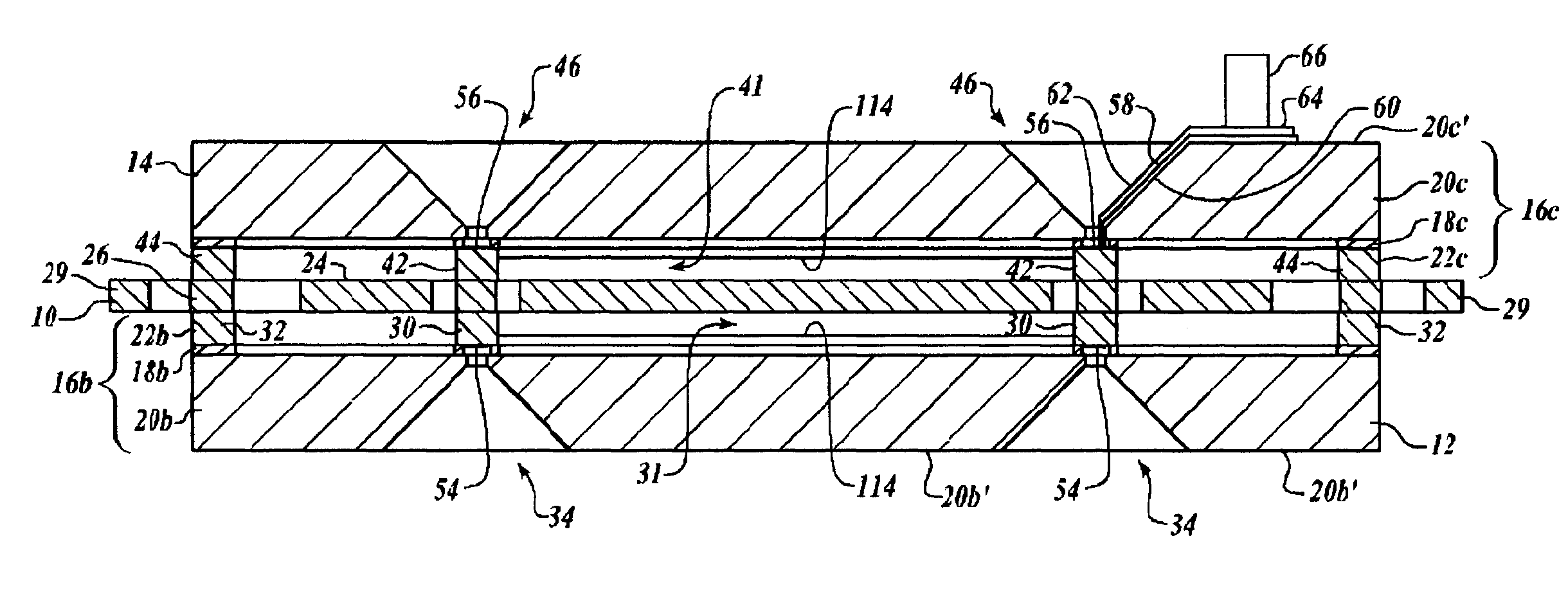
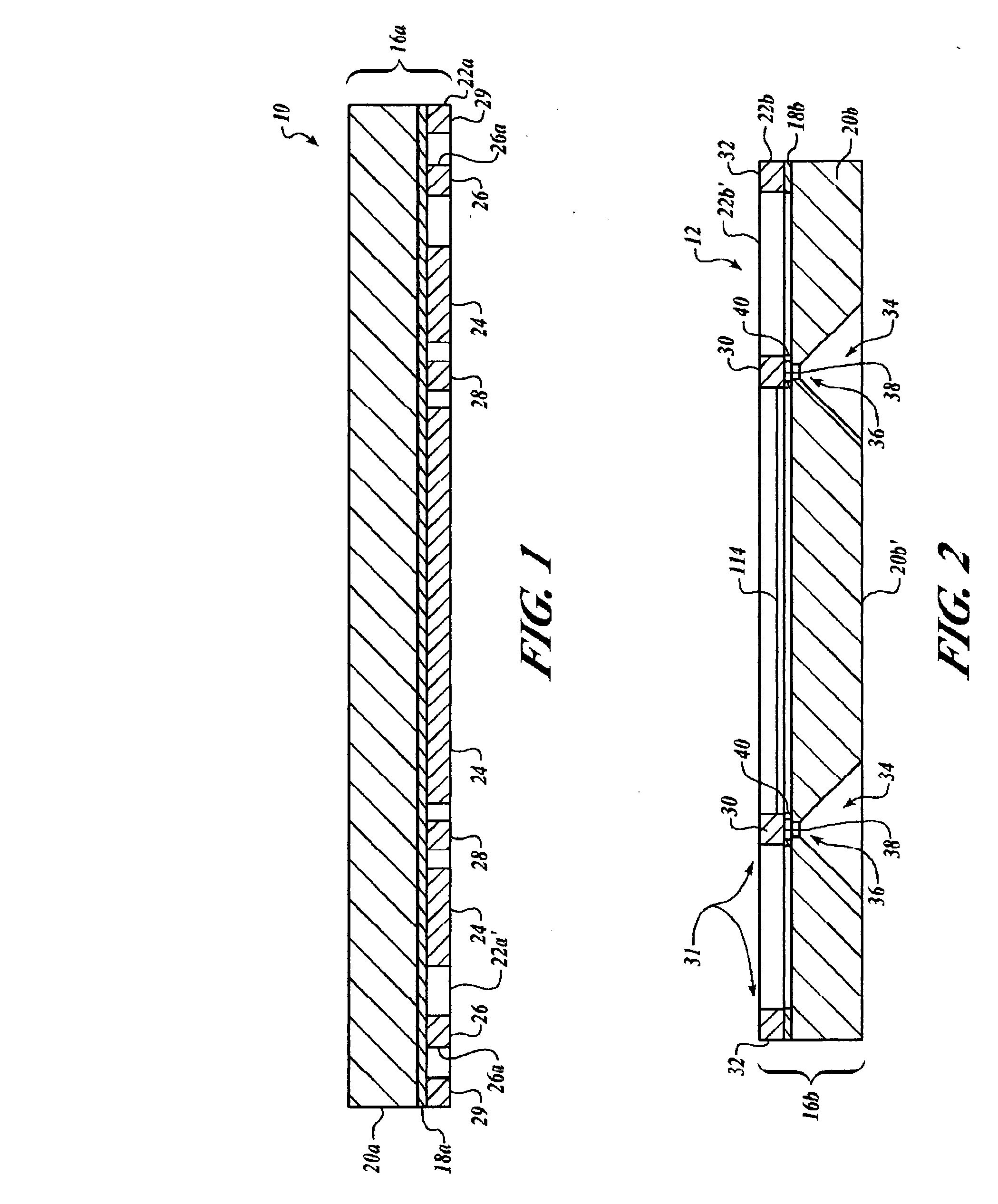
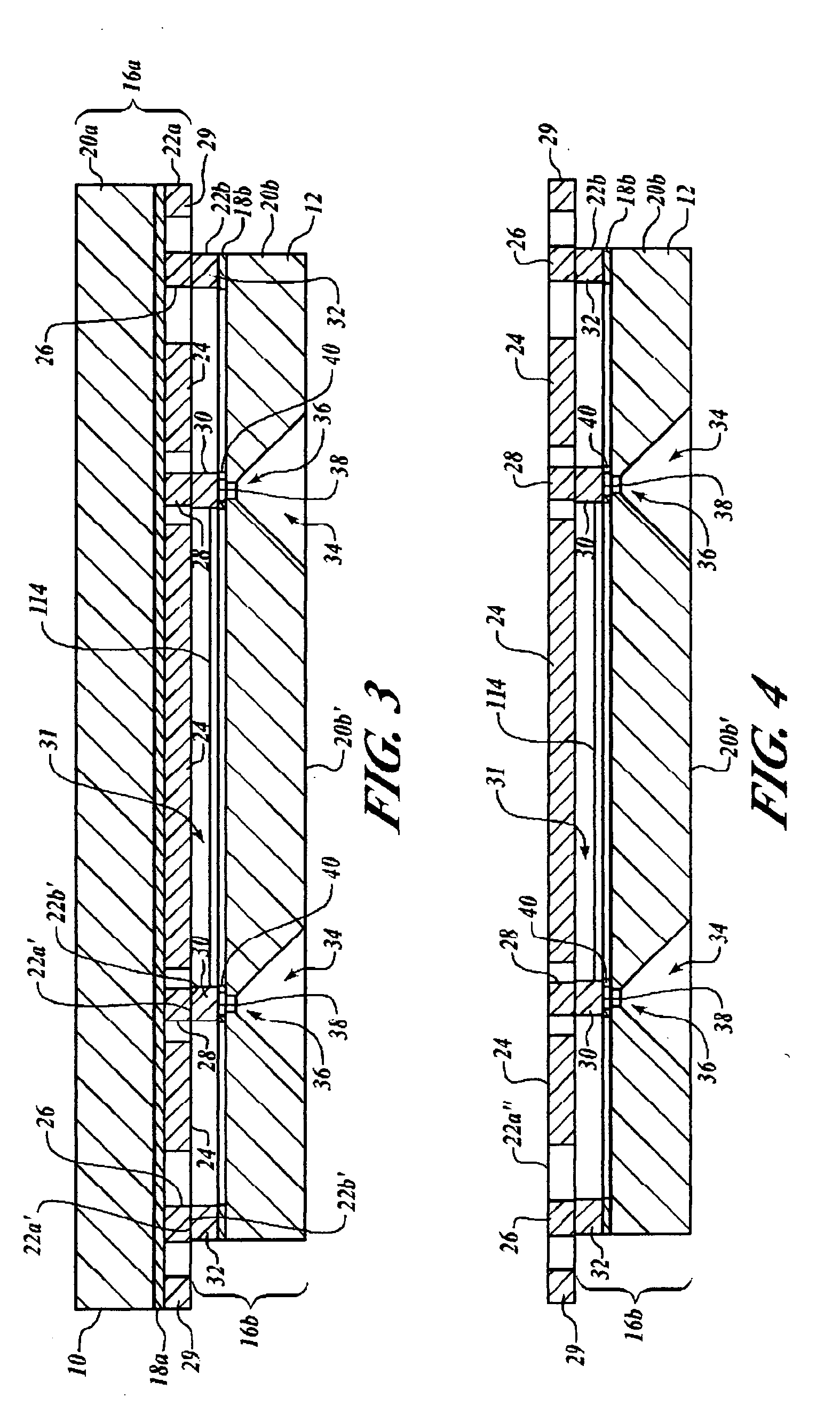
[0055] The Figures illustrate the method of the present invention for fabricating a sensor architecture based on bulk machining of Silicon-On-Oxide (SOI) wafers and fusion bond joining that produces a symmetric, nearly all-silicon, hermetically sealed, microelectromechanical system (MEMS) inertial device 1, such as an electrostatic accelerometer or Coriolis rate gyro device, operated in either open-loop or closed-loop modes.

[0056] The architecture of the present invention includes a device sensor mechanism 10 and first and second silicon cover plates 12, 14 bonded to opposite faces of the device sensor mechanism 10. The device sensor mechanism 10 and silicon cover plates 12, 14 are formed in different SOI wafer elements of a type that is generally commercially available. Each wafer element includes a buried dielectric layer having a thickness of from about 0.5 to 2.0 microns that is sandwiched between a relatively thicker...


PUM


Abstract

An apparatus and method for sensor architecture based on bulk machining of Silicon-On-Oxide wafers and fusion bonding that provides a symmetric, nearly all-silicon, hermetically sealed MEMS device having a sensor mechanism formed in an active semiconductor layer, and opposing silicon cover plates each having active layers bonded to opposite faces of the sensor mechanism. The mechanism is structured with sensor mechanical features structurally supported by at least one mechanism anchor. The active layers of the cover plates each include interior features structured to cooperate with the sensor mechanical features and an anchor structured to cooperate with the mechanism anchor. A handle layer of each cover plate includes a pit extending there through in alignment with the cover plate anchor. An unbroken rim of dielectric material forms a seal between the cover plate anchor and the pit and exposes an external surface of the cover plate anchor.

Description

FIELD OF THE INVENTION [0001] The present invention relates to micro-machined sensor devices and methods, and in particular to micro-machined accelerometers using a Silicon-On-Insulator (SOI) architecture. BACKGROUND OF THE INVENTION [0002] Microelectromechanical system or “MEMS” devices are generally well-know. In the most general form, MEMS consist of mechanical microstructures, microsensors, microactuators and electronics integrated in the same environment, i.e., on a silicon chip. MEMS is an enabling technology in the field of solid-state transducers, i.e., sensors and actuators. The microfabrication technology enables fabrication of large arrays of devices, which individually perform simple tasks but in combination can accomplish complicated functions. Current applications include accelerometers, pressure, chemical and flow sensors, micro-optics, optical scanners, and fluid pumps. For example, one micromachining technique involves masking a body of silicon in a desired pattern,...

Claims


Application Information

Patent Timeline
IPC IPC(8): H01L29/82
CPCG01C19/5719G01P1/023H01L2924/1461H01L2224/48091H01L2924/10253H01L2924/01322H01L2924/01014H01L2924/01013H01L2224/45144G01P15/18G01P15/125G01P15/0802H01L2924/00014H01L2924/00
Inventor LAFOND, PETER H.YU, LIANZHONG
Owner HONEYWELL INT INC
Why Eureka
Try Eureka