Wiring board and production method thereof

Inactive Publication Date: 2006-07-27
HITACHI CABLE
View PDF18 Cites 35 Cited by
  • Summary
  • Abstract
  • Description
  • Claims
  • Application Information

AI Technical Summary

Benefits of technology

[0011] The present invention allows high-density wiring with a controlled shape to be formed without using a resist. The angle between the wiring side and the s

Problems solved by technology

These steps involve high cost due to the use of chemicals and the treatment of waste liquid.
In addition, the large number of the steps cause a long processing time.
Thus, the process of masking by the resist film has been a bottleneck in producing wiring boards with low cost in a short time.
For example, the method in which a metal seeding solution layer is formed on a substrate surface and exposed to light to form a metal seed layer and then plating or the like is performed to form a metal film has difficulty in forming wiring with higher density since the shape of the plated film serving as wiring is not sufficiently considered.

Method used


Image

  • Wiring board and production method thereof
  • Wiring board and production method thereof
  • Wiring board and production method thereof

Examples


example 1

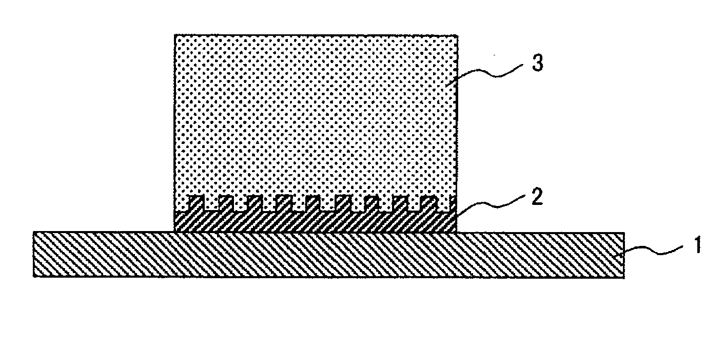
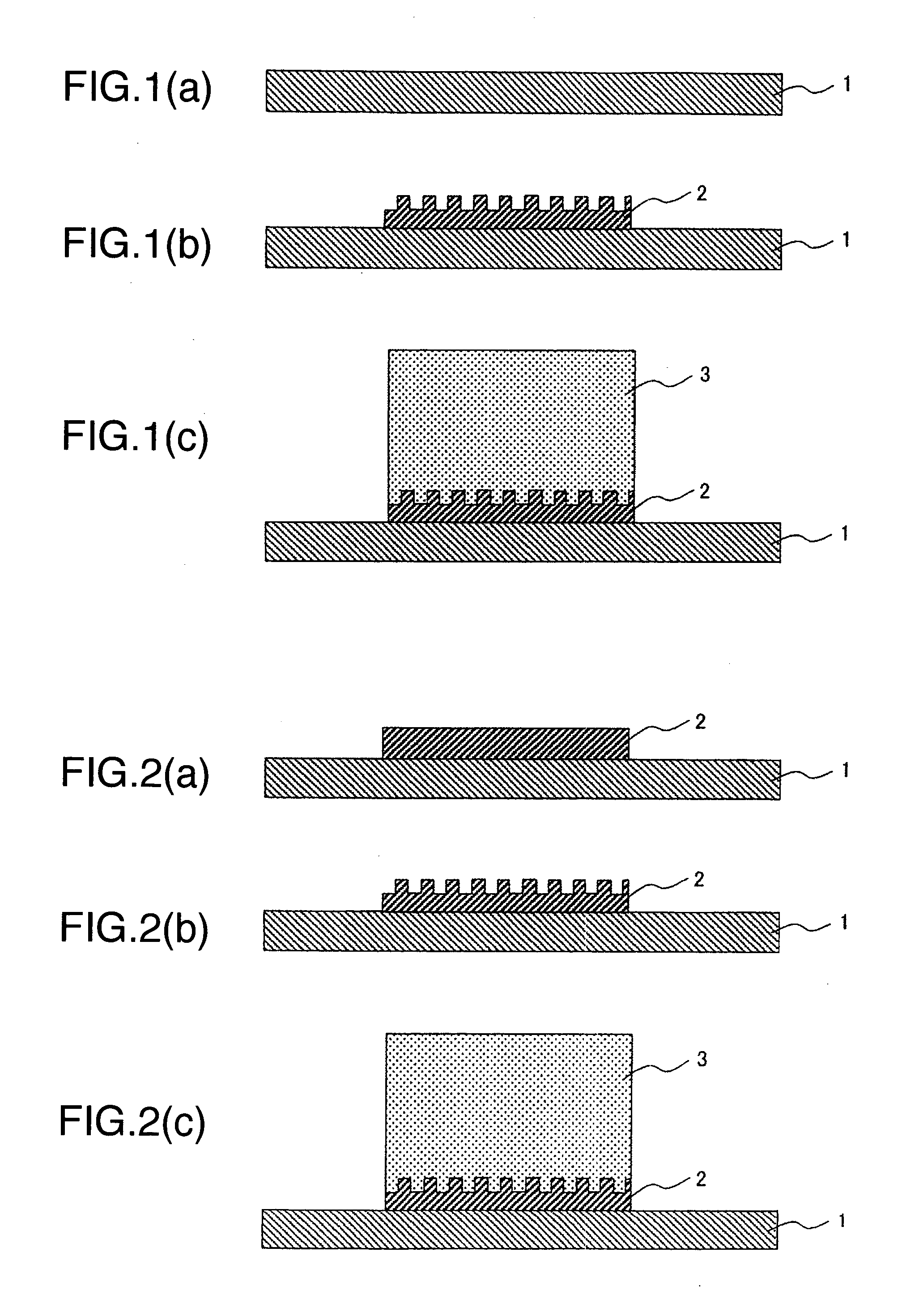
[0044] A solution containing dispersed silver particles with an average diameter of 20 nm was sprayed with an ink jet technique onto a surface of an insulating substrate 1 (Kapton EN made by Du Pont-Toray Co., Ltd.) made of polyimide film with a thickness of 25 μm shown in FIG. 1(a) to form a metal seed layer 2 with a wiring width of 20 μm and a thickness of 0.2 μm as shown in FIG. 1(b). Then, the insulating substrate was heated to a temperature of 200° C. to fuse the silver particles. As the insulating substrate, it is possible to use not only the polyimide but also a resin of polyester, class epoxy, phenol, and aramid, ceramics, and glass. As the particles, it is possible to use metal particles of platinum, gold, copper, nickel, tin and the like, other than silver. The roughness on the surface of the metal seed layer formed by the silver particles was measured with a surface roughness measuring apparatus. The measurement showed that the surface roughness of the metal seed layer ha...

example 2

[0048] A metal seed layer 2 with a wiring width of 10 μm was formed as shown in FIG. 2(a) through a mask with a sputtering technique on a surface of an insulating substrate 1 (Upilex S made by Ube Industries Ltd.) made of polyimide film with a thickness of 25 μm shown in FIG. 2(a). The metal seed layer was made of two layers: a nickel film with a thickness of 0.01 μm formed on the substrate and a copper film with a thickness of 0.5 μm formed on the nickel film. As the metal seed layer, it is possible to use not only the stacked film of nickel and copper but also a stacked film of chromium and copper. Then, copper roughening processing was performed to form a roughened shape on the surface of the copper film as shown in FIG. 2(b). The metal seed layer in FIG. 2(b) is made of the two layers, although not shown. The copper roughening processing was performed by using MultiBond made by Nippon MacDermid Co., Inc. in accordance with steps shown in Table 3. As a solution used copper roughe...

example 3

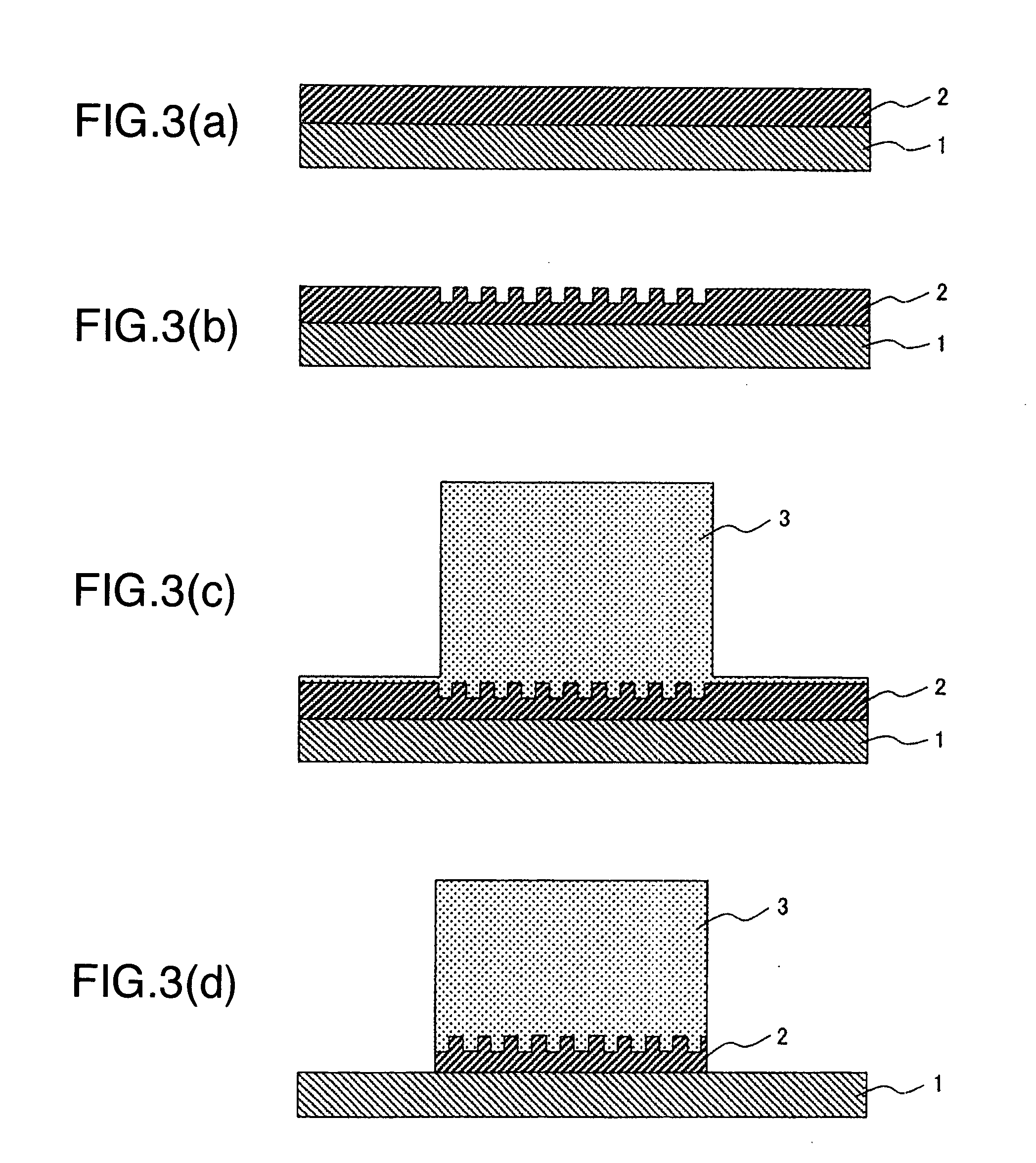
[0051] As shown in FIG. 3(a), a nickel film with a thickness of 0.1 μm formed on a surface of an insulating substrate 1 made of glass epoxy resin and a copper film with a thickness of 1.0 μm was formed with the sputtering technique on the nickel film. Next, copper roughening processing was performed to form a rough area in the portion of the copper surface on which wiring was to be formed, thereby providing the shape shown in FIG. 3(b). The rough area was formed with sandblast. The sandblast was performed by spraying alumina particles onto the copper surface through a mask pattern with a wiring width of 8 μm. The roughened shape on the copper surface after the sandblast processing was measured with a surface roughness measuring apparatus. The measurement showed that the surface roughness of the metal seed layer had an arithmetic average roughness Ra (defined in JIS B0601) of 0.4 μm and an average length of a roughness curve element RSm of 1.1 μm. Electroplating was performed immedia...


PUM


Abstract

It is an object of the present invention to provide a wiring board having high-density wiring with a controlled shape without masking by a resist film and a production method thereof. In the present invention, the production method of a wiring board having copper wiring on an insulating substrate includes the steps of forming a metal seed layer on the insulating substrate, the metal seed layer having a roughened shape in a portion on which the copper wiring or a bump is to be formed, and forming an electroplated film of copper or an alloy of copper through electroplating on the portion of the metal seed layer having the roughened shape. A substance for suppressing the plating reaction is added to a plating bath to provide an angle of 90 degrees or smaller between a surface of the insulating substrate and a side of the electroplated film.

Description

INCORPORATION BY REFERENCE [0001] The present application claims priority from Japanese application JP2005-019437 filed on Jan. 27, 2005, the content of which is hereby incorporated by reference into this application. BACKGROUND OF THE INVENTION [0002] The present invention relates to a wiring board having a wiring made of copper or an alloy of copper, and to a production method thereof. [0003] Electronic devices with smaller size, lighter weight, and lower cost are needed increasingly year after year. This requires wiring boards used in those electronic devices to have high-density wiring formed with low cost in order to achieve smaller size and lighter weight. Production methods of wiring boards can be broadly classified into two: a subtractive method and an additive method. In the subtractive method, an etching resist is formed on a copper foil applied to a substrate and the copper is etched away except the portions which will serve as wiring, thereby forming wiring. In the addit...

Claims


Application Information

Patent Timeline
IPC IPC(8): H01L23/48H01L21/44
CPCH01L21/4846H01L23/49838H01L2924/09701H05K3/108H05K3/241H05K3/382H05K3/388H01L2924/0002H01L2924/00
Inventor HABA, TOSHIOYOSHIDA, HIROSHIAKAHOSHI, HARUOSUZUKI, HITOSHICHINDA, AKIRA
Owner HITACHI CABLE
Why Eureka
Try Eureka