Substrate processing apparatus and substrate processing method

a technology for processing apparatus and substrate, which is applied in the direction of photomechanical apparatus, instruments, coatings, etc., can solve the problems of difficult maintenance work for the conveyance chamber, the size of the apparatus cannot be decreased, and the work efficiency of maintenance work is reduced, so as to improve the yield the throughput of the treatment of the substrate under treatment can be improved, and the size of the apparatus can be reduced

Inactive Publication Date: 2006-08-03
TOKYO ELECTRON LTD
View PDF5 Cites 30 Cited by
  • Summary
  • Abstract
  • Description
  • Claims
  • Application Information

AI Technical Summary

Benefits of technology

[0061] Thus, according to the present invention, the size of the apparatus can be reduced. In addition, the throughput of the treatment of a substrate under treatment can be improved and the yield of the substrate under treatment can be improved. According to the present inv

Problems solved by technology

Thus, as a problem of this apparatus, the size of the apparatus cannot be decreased.
In addition, since the conveyance chamber is disposed around other treatment chambers, it is difficult to perform maintenance work for the conveyance chamber.
Thus, the work efficiency of the maintenance work lowers and the hour cost for the maintenance work increases.
Thus, the efficiency of a treatment process for a semiconductor wafer in the whole system cannot be improved.
Although the foregoing second apparatus (Patent Document 2) is an apparatus that inline-connects the resist treatment device and the exposure treatment device that performs an exposure treatment for the semiconductor wafer that has been coated with a resist file, the apparatus lacks for a concept of which the exposure treatment device performs the treatment under a reduced pressure atmosphere.
Thus,

Method used


Image

  • Substrate processing apparatus and substrate processing method
  • Substrate processing apparatus and substrate processing method
  • Substrate processing apparatus and substrate processing method

Examples


first embodiment

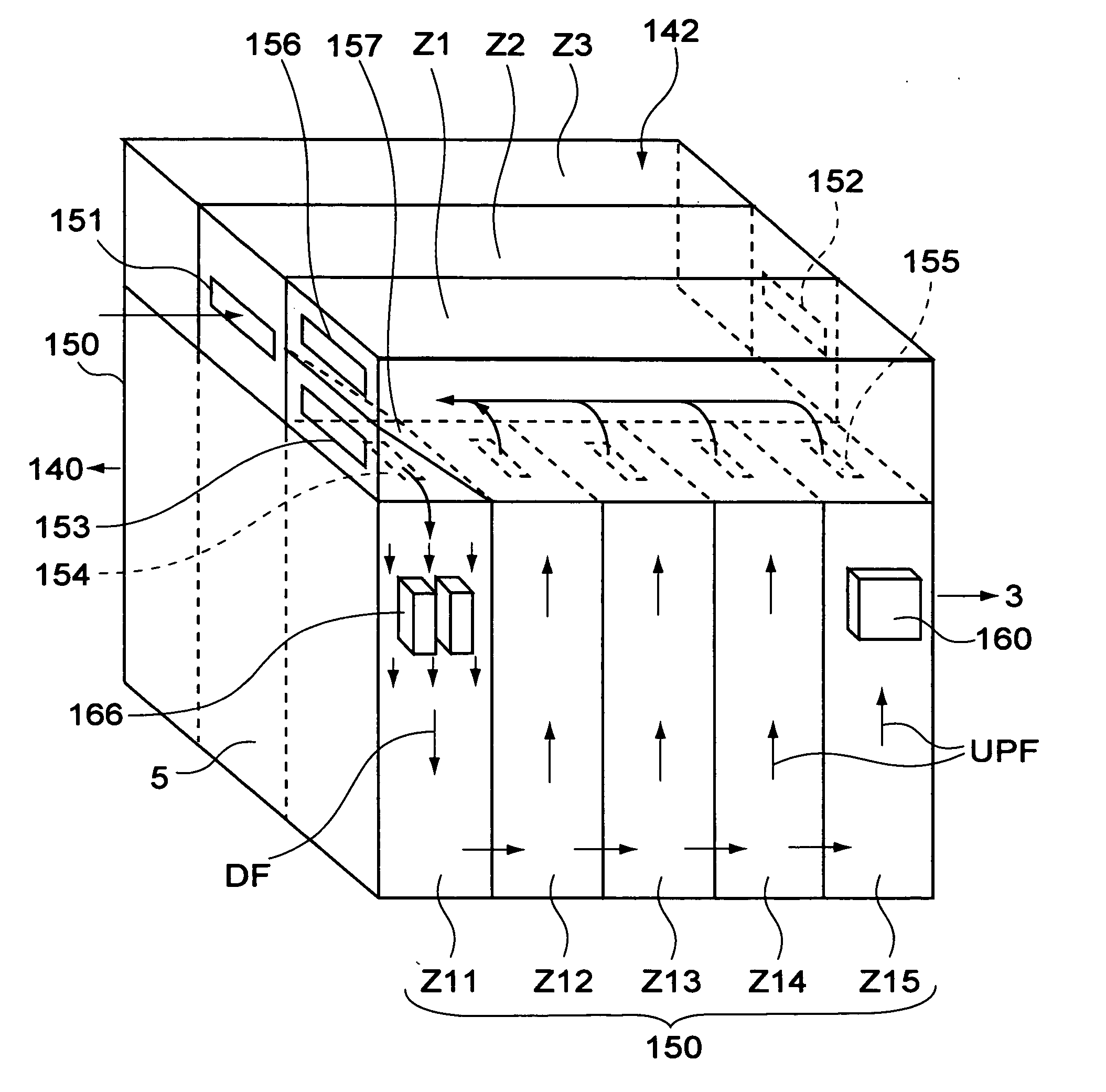
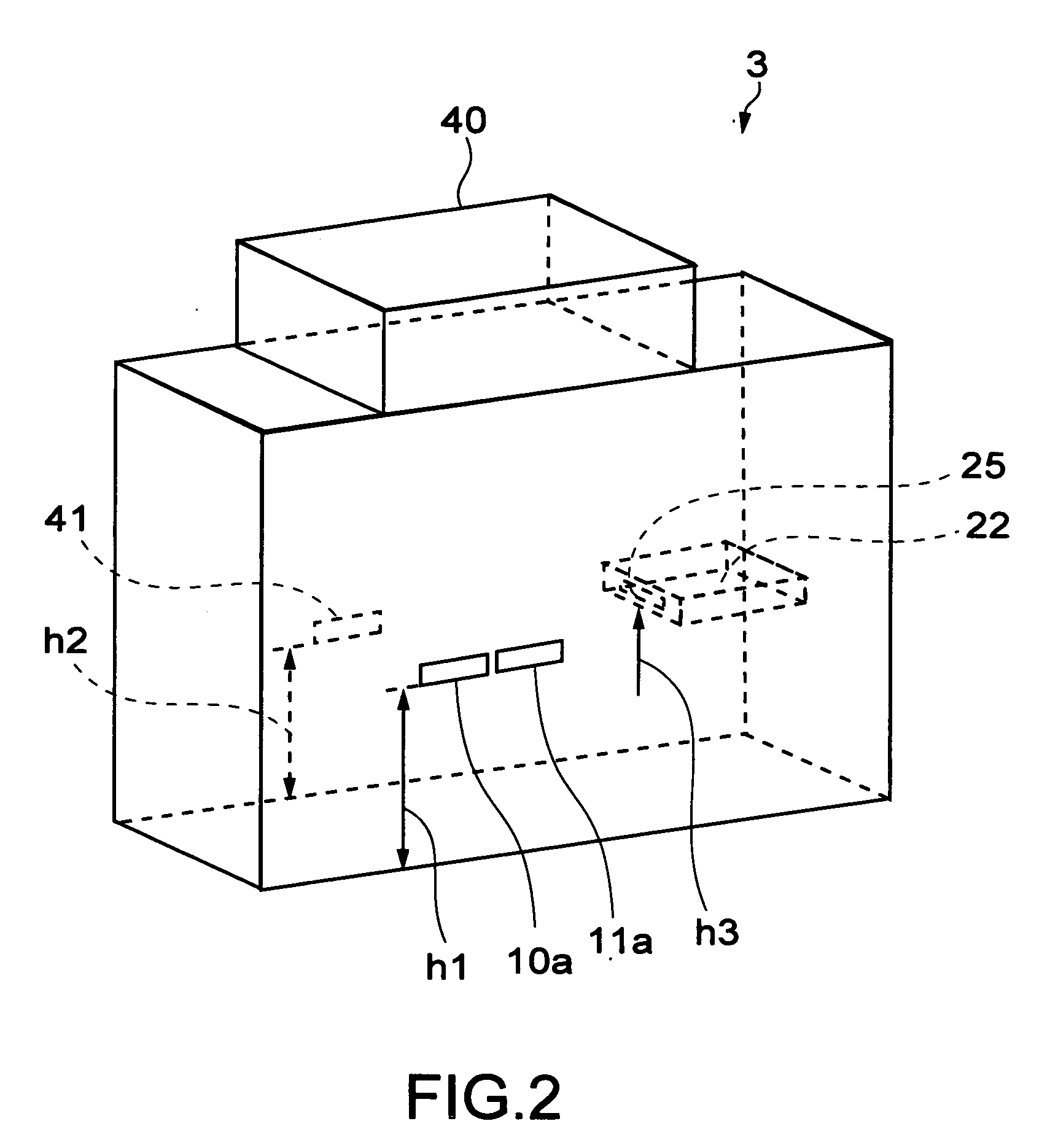
[0121]FIG. 1 is a schematic diagram showing the structure of a system of an exposure device as an example of a substrate treatment apparatus according to an embodiment of the present invention. The system of the exposure device 1 can be freely inline-connected to another device such as a resist treatment device 2 (on C / D side in FIG. 1). The resist treatment device 2 has a coating device (coater: COT) that applies resist solution onto a treatment surface of a substrate under treatment for example a semiconductor wafer and a development device (developer: DEV) that develops a resist film formed on the treatment surface of the semiconductor wafer W. In addition, the exposure device 1 has an air aligner section 3 (S1 in FIG. 1) that has a linear space portion as a first unit (interface section) that conveys the semiconductor wafer W under a normal atmosphere (non-reduced pressure atmosphere) and an exposure treatment section 5 (S2 in FIG. 1) as a second unit that has an exposure treatm...

second embodiment

[0225]FIG. 28A and FIG. 28B show the structure of a wafer rotation position detection apparatus according to a second embodiment of the present invention. A wafer rotation position detection apparatus 1001 according to this embodiment has a chamber 1003, a stage 1005 that is disposed in the chamber 1003 and on which a wafer 1100 is placed, a photographing device 1007 that is composed of for example a CCD camera that detects the rotation position of the wafer, and an image process device 1009 that processes image data captured by the photographing device 1007. The image process device 1009 has a first visual field setting section 1009a, a second visual field setting section 1009b, a second visual field moving section 1009c, a notch representative position detection section 1009d, an edge position detection section 1009e, and a wafer rotation amount calculation section 1009f.

[0226] Next, with reference to FIG. 29 to FIG. 31, the operation of the wafer rotation position detection appa...

third embodiment

[0238] Next, with reference to FIG. 32 to FIG. 34, a wafer rotation position detection apparatus according to a third embodiment of the present invention will be described. The wafer rotation position detection apparatus according to this embodiment has a structure of which the image process device 1009 of the wafer rotation position detection apparatus according to the second embodiment shown in FIG. 2 is replaced with an image process device 1009A shown in FIG. 32. FIG. 32 is a block diagram showing the structure of the image process device 1009A according to the third embodiment. The image process device 1009A has a first detection frame setting section 1009Aa, a second detection frame setting section 1009Ab, a first detection frame moving section 1009Ac, an edge position detection section 1009Ad, and a wafer rotation amount calculation section 1009Ae.

[0239] Next, with reference to FIG. 33 and FIG. 34, the operation of the wafer rotation position detection apparatus according to...


PUM

PropertyMeasurementUnit
Temperatureaaaaaaaaaa
Pressureaaaaaaaaaa
Heightaaaaaaaaaa

Abstract

A substrate treatment apparatus that treats a substrate under treatment has an interface section, a substrate loading/unloading section, a reduced pressure atmosphere conveyance chamber, and an exposure treatment chamber. The interface section has a conveyance mechanism that can freely load and unload the substrate under treatment from another device into the apparatus or vice versa. The substrate under treatment can be loaded and unloaded into and from the substrate loading/unloading section in one direction by the conveyance mechanism of the interface section. The reduced pressure atmosphere conveyance chamber is disposed adjacent to and perpendicular to the direction of the substrate loading/unloading section and has a conveyance mechanism that conveys the substrate under treatment under a reduced pressure atmosphere. The exposure treatment chamber is disposed adjacent to and in parallel with the direction of the reduced pressure atmosphere conveyance chamber and performs an exposure treatment for the substrate under treatment.

Description

BACKGROUND OF THE INVENTION [0001] 1. Field of the Invention [0002] The present invention relates to a substrate treatment apparatus and a substrate treatment method. [0003] 2. Description of the Related Art [0004] An apparatus that has a loader, a conveyance device thereof, a load lock chamber, a conveyance chamber, a conveyance device thereof, and a reduced pressure atmosphere treatment chamber is known. In this apparatus, the conveyance device of the loader that conveys a semiconductor wafer under a normal atmosphere. The conveyance device conveys the semiconductor wafer to the load lock chamber that changes the inner atmosphere from the normal atmosphere to a reduced pressure atmosphere. The conveyance device of the conveyance chamber transfers the semiconductor wafer from the load lock chamber to the reduced pressure atmosphere treatment chamber. This apparatus is disclosed for example in Patent Document 1. In addition, an apparatus that inline-connects a resist treatment devic...

Claims


Application Information

Patent Timeline
IPC IPC(8): C23C16/00H01L21/31H01L21/469
CPCG03F7/7075G03F7/70808G03F7/70991G03F9/7003G03F9/7011H01L21/67017H01L21/67225H01L21/67248H01L21/67748H01L21/68H01L21/681
Inventor SHINOZAKI, HIROYUKIKOJIMA, YASUSHIAIYOSHIZAWA, SHUNICHITSUKAMOTO, KIWAMU
Owner TOKYO ELECTRON LTD
Why Eureka
Try Eureka