Group III nitride-based compound semiconductor light-emitting device and method for producing the same

a compound semiconductor and light-emitting device technology, applied in the field of group iii nitride-based compound semiconductor light-emitting devices, can solve the problems of inability to realize four-component alingans having high crystallinity, and inability to achieve excellent emission intensity and output intensity, etc., to prevent the generation of edge dislocations, enhance crystallinity, and reduce the effect of misfit dislocation

Active Publication Date: 2006-08-03
TOYODA GOSEI CO LTD
View PDF4 Cites 24 Cited by
  • Summary
  • Abstract
  • Description
  • Claims
  • Application Information

AI Technical Summary

Benefits of technology

[0031] According to the first aspect of the present invention, generation of misfit dislocations at a region in the vicinity of the interface of the well layer can be suppressed, thereby preventing generation of edge dislocations originating from misfit dislocations and enhancing crystallinity. As a result, device characteristics such as emission intensity, output intensity, and service life of the produced semiconductor device can be enhanced. The effect is particularly remarkable when a three- or two-component semiconductor of high crystallinity is employed.

Problems solved by technology

However, four-component AlInGaN having high crystallinity is not realized.
Thus, even though lattice mismatch is mitigated, excellent emission intensity and output intensity, which are the most important characteristics of light-emitting devices, cannot be attained.
Furthermore, since the well layer is generally very thin, the In composition is difficult to vary in the well layer.
However, the document neither discloses nor suggests the mode of application of the structure and applicability thereof to the light-emitting layer.

Method used


Image

  • Group III nitride-based compound semiconductor light-emitting device and method for producing the same
  • Group III nitride-based compound semiconductor light-emitting device and method for producing the same
  • Group III nitride-based compound semiconductor light-emitting device and method for producing the same

Examples


example 1

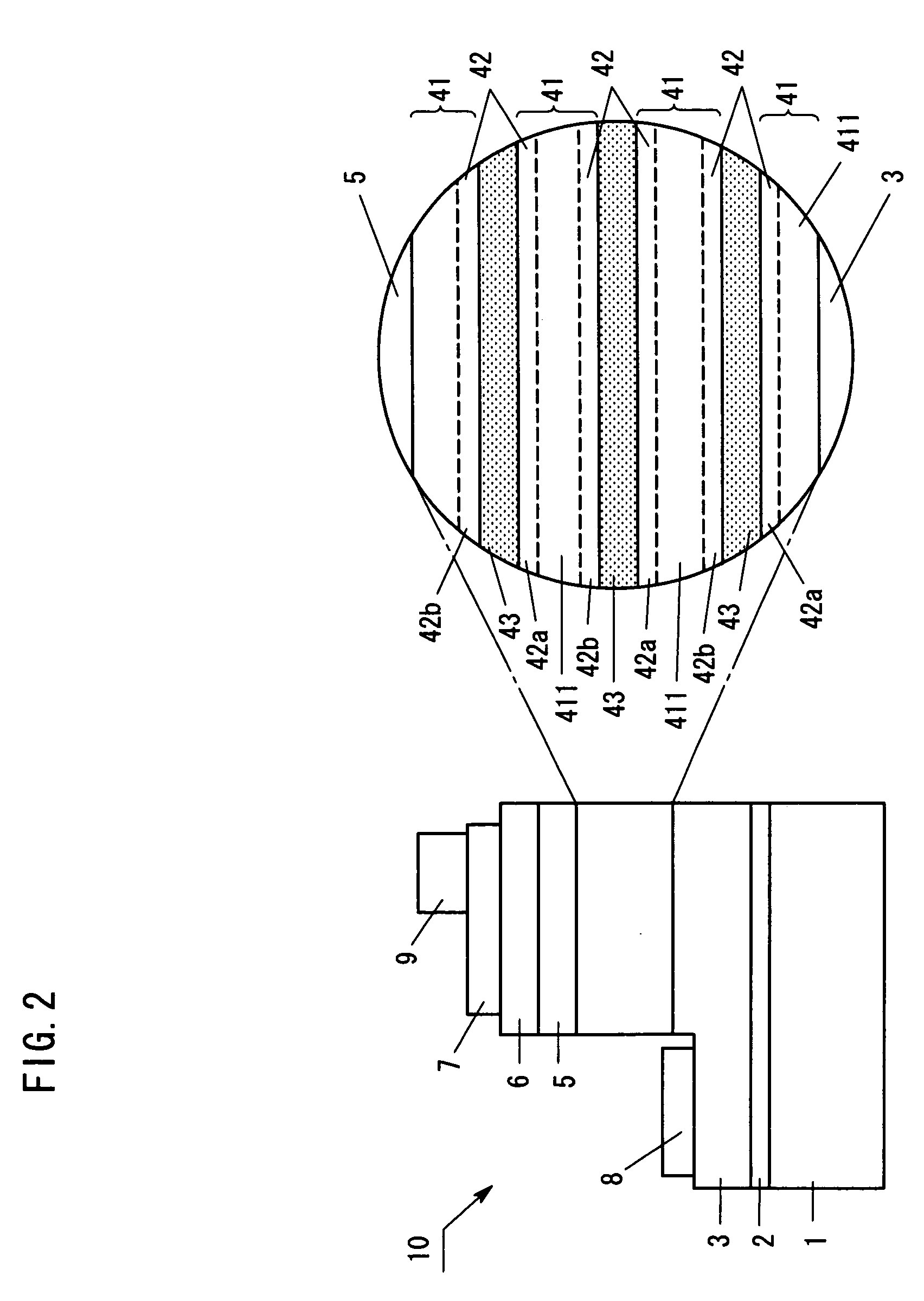
[0044]FIG. 2 is a schematic cross-sectional view of a light-emitting device 10 fabricated from Group III nitride-based compound semiconductors. In the device, light is extracted through the top surface on the semiconductor layer formed on a sapphire substrate 1. On the substrate 1, an AlN buffer layer 2 (thickness: about 25 nm) and a high-carrier-concentration layer 3 (thickness: about 4.0 μm) formed of silicon (Si)-doped GaN are sequentially formed. On the high-carrier-concentration layer 3, there is formed a multiple quantum well layer 4 in which barrier layers 41 (thickness: about 8 nm) and In0.1Ga0.9N well layers 43 (thickness: about 3 nm) are alternatingly stacked. Each barrier layer 41 includes a main region 411 formed of Al0.1Ga0.9N and an interface region 42 (thickness: about 1.5 nm) which is in contact with the well layer 43. In an interface region 42a underneath the well layer 43, the Al composition of Al0.1Ga0.9N in the main region 411 continuously decreases toward the up...

example 2

[0061] In Example 1, the composition of the interface region 42a in contact with the lower surface of the well layer 43 is varied from AlGaN, via GaN, to InGaN. Alternatively, the composition of the interface region 42a may be varied from AlGaN to GaN, and this compositional variation is also effective. In the case, the following procedure was employed. After formation of the high-carrier-concentration layer 3, the temperature of the substrate 1 was adjusted to 900° C., and N2, NH3, TMA, and TMG were supplied to the chamber, to thereby form an Al0.1Ga0.9N main region 411 (thickness: about 5 nm). The TMA feed rate was continuously decreased to 0 with lowering the temperature of the substrate 1, to thereby form a region 42a (thickness: about 1.5 nm) which is in contact with the lower surface of the well layer 43. During the course of temperature lowering, the TMA feed rate was controlled to 0 when the temperature of the substrate 1 reached 600° C. In Example 2, a first barrier layer 4...

example 3

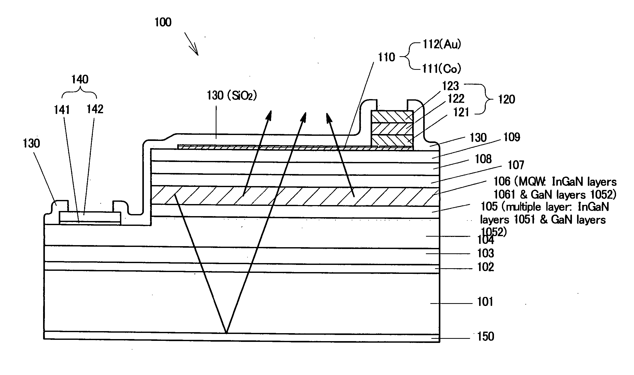
[0079]FIG. 4 is a schematic cross-sectional view of a Group III nitride-based compound semiconductor light-emitting device 100 of Example 3 of the present invention. As shown in FIG. 4, in the semiconductor light-emitting device 100, an aluminum nitride (AlN) buffer layer 102 (thickness: about 10 nm), a non-doped GaN layer 103 (thickness: about 2 μm), and an n-type contact layer 104 (high-carrier-concentration n+ layer) (thickness: about 3 μm) formed of silicon (Si)-doped GaN with a dopant amount of 5×10¹⁸ / cm3 were sequentially formed on a sapphire substrate 101 (thickness: about 300 μm).

[0080] On the n-type contact layer 104, a multilayer 105 (thickness 40 nm) and a light-emitting layer 106 of a multiple quantum well structure were sequentially formed, the multilayer 105 comprising stacked 20 pairs of a non-doped In0.1Ga0.9N layer 1051 (thickness: 1 nm) and a non-doped GaN layer 1052 (thickness: 1 nm), and the light-emitting layer 106 comprising stacked 6 pairs of a non-doped In0....


PUM


Abstract

The invention relates to a Group III nitride-based compound semiconductor light-emitting device having a well layer, a first layer formed on one surface of the well layer, a second layer formed on the other surface of the well layer, a first region provided in the vicinity of the interface between the first layer and the well layer, and a second region provided in the vicinity of the interface between the second layer and the well layer, wherein the first and second regions are formed such that the lattice constants of the first and second layers approach the lattice constant of the well layer. The invention also relates to a method for producing a Group III nitride-based compound semiconductor light-emitting device having a light-emitting layer of a single or multiple quantum well structure including at least an indium (In)-containing well layer, wherein, during formation of the well layer through vapor growth, an In source is fed through a procedure including: initiating feeding of the In source at a minimum feed rate; subsequently, elevating the In source feed rate to a target feed rate; maintaining the feed rate at the target feed rate; and subsequently, lowering the feed rate from the target feed rate to the minimum feed rate, and a Group III source other than the In source is fed at a constant feed rate from initiation of feeding of the In source to termination of the feeding.

Description

BACKGROUND OF THE INVENTION [0001] 1. Field of the Invention [0002] The present invention relates to a Group III nitride-based compound semiconductor light-emitting device having a quantum well structure. [0003] The invention also relates to a method for producing a Group III nitride-based compound semiconductor device or light-emitting device, and more particularly, to a method for growing an indium-containing Group III nitride-based compound semiconductor layer. [0004] 2. Description of the Related Art [0005] Conventionally, Group III nitride-based compound semiconductor light-emitting devices employ a multiple quantum well (MQW) structure in which layers having different bandgap energies are alternatingly stacked at a predetermined number of repetitions of a stacked layer cycle. Examples include a blue-light-emitting diode (LED) and a green-light-emitting LED, employing a multiple quantum well (MQW) structure in which well layers In0.2Ga0.8N (thickness: 2.5 nm) and barrier layers...

Claims


Application Information

Patent Timeline
Patent Type & Authority Applications(United States)
IPC IPC(8): H01L33/00H01L33/06H01L33/32
CPCB82Y20/00H01L33/06H01L33/32
Inventor TAKI, TETSUYANARUKAWA, MITSUHISAAOKI, MASATOOKUNO, KOJITOYODA, YUSUKENISHIJIMA, KAZUKIYAMADA, SHUHEI
Owner TOYODA GOSEI CO LTD
Why Eureka
Try Eureka