Electronic device, method for manufacturing electronic device, contact hole of electronic device, method for forming contact hole of electronic device

a technology of electronic devices and contact holes, which is applied in the direction of semiconductor/solid-state device details, instruments, coatings, etc., can solve the problems of increasing manufacturing costs, increasing manufacturing costs, and difficult to achieve satisfactory and reliable electric connection of electrodes

Inactive Publication Date: 2006-08-03
RICOH KK
View PDF9 Cites 28 Cited by
  • Summary
  • Abstract
  • Description
  • Claims
  • Application Information

AI Technical Summary

Benefits of technology

[0057] It is a general object of the present invention to provide an electronic device, a method of manufacturing an electronic device, a contact hole of an electronic device, a method of forming a contact hole of an e...

Problems solved by technology

This typical method, however, requires many steps, and results in an increase of manufacturing cost.
However, the related art case shown in Japanese Laid-Open Patent Application No. 2002-261048 requires the steps of applying a coating of insulation material on a substrate, applying a coating of organo-siloxane on the substrate, and exposing the substrate, since organo-siloxane itself does not have an insulating property.
Therefore, it is difficult to attain satisfactory and reliable electric connection of electrodes.
These required processes result in increase of manufacturing cost.
Furthermore, since the method requires heating under a high temperature of 400° C., the materials to be used for the substrate, for example, is limited.
In the related art case shown in Japanese Laid-Open Patent Application No. 7-86600, the organic semiconductor material layer may be damaged in a case where an interlayer insulation film is deposited by using an organic solution having little polarity (e.g. toluene, THF, xylene).
In the related art case shown in Japanese Laid-Open Patent Application No. 5-36627, althou...

Method used


Image

  • Electronic device, method for manufacturing electronic device, contact hole of electronic device, method for forming contact hole of electronic device
  • Electronic device, method for manufacturing electronic device, contact hole of electronic device, method for forming contact hole of electronic device
  • Electronic device, method for manufacturing electronic device, contact hole of electronic device, method for forming contact hole of electronic device

Examples


first embodiment

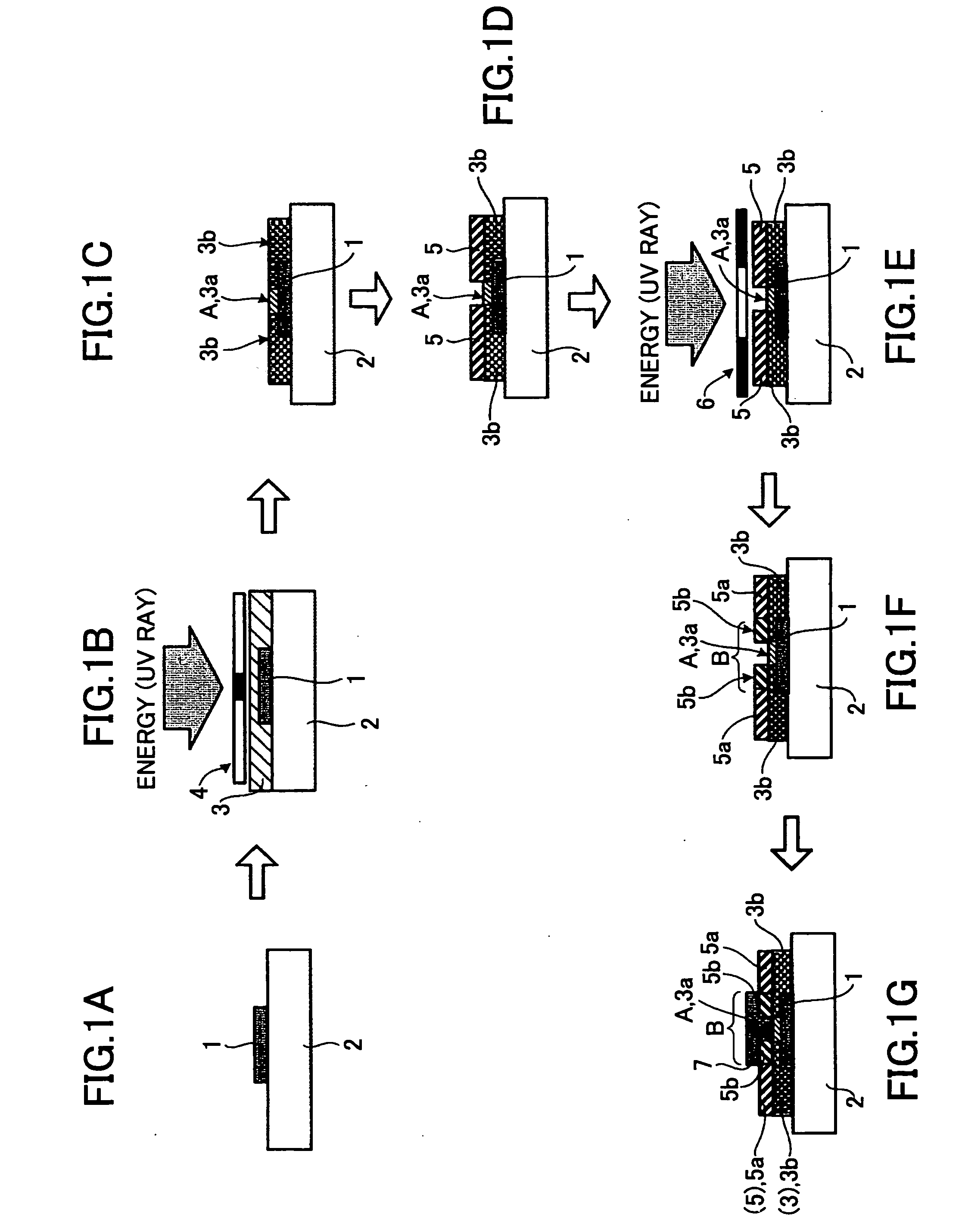
[0098] A method of manufacturing an electronic device and a configuration of an electronic device manufactured by the method according to the first embodiment of the present invention are described with reference to FIGS. 1A-1G.

[0099] First, a first conductive material layer 1 is formed by depositing / forming a first conductive material on a substrate 2 (See FIG. 1A). Then, a patterning layer 3, which is formed of a material having a changing critical surface tension, is selectively deposited / formed on the first conductive material layer 1 by applying energy (e.g. UV rays) thereto (See FIG. 1B) Then, a first portion A of the patterning layer 3 (i.e. low surface energy part 3a), which has a critical surface tension that is different from that of other portions of the patterning layer 3 (i.e. high surface energy part 3b), is formed at the part where the first conductive material layer 1 electrically contacts a second conductive material layer 7 (described below) (See FIG. 1C). Then, a...

second embodiment

[0170] Next, the second embodiment of the present invention is described with reference to FIGS. 10, 14 and 19.

[0171]FIG. 10 is a wiring diagram of a liquid crystal display element 61. The liquid crystal display element 61 is an example of a display element including an electronic device (including as contact hole 62 and pixel electrode 63 as shown in FIG. 14) obtained by performing the contact hole / electronic device manufacturing method according to the first embodiment of the present invention. FIG. 14 shows a configuration of a display part of a display device 60 including the liquid crystal display element 61 shown in FIG. 14.

[0172]FIG. 19 is a cross-sectional view of a configuration of another display device 700 including a display element 710. The display element 710 is another example of a display element including an electronic device (including as contact hole 712 and pixel electrode 702 as shown in FIG. 19) obtained by performing the contact hole / electronic device manufa...

example 1

[0178] Next, a first example of an electronic device according to an embodiment of the present invention is described with reference to the process shown in FIGS. 1A to 1G.

[0179] In FIG. 1A, a Cr / Au film is formed on the substrate 2 (in this example, a glass substrate) by depositing a Cr / Au electrode (i.e. first conductive material layer 1) of a prescribed pattern by using a metal exposure mask (not shown). The thickness of the Cr / Au film (electrode) in this example is approximately 100 nm. Then, a mixed solvent having a precursor (which has a structure expressed with the below-given Chemical Formula 11 and the above-described Chemical Formula 2 subsequent to a burning process) dissolved therein is applied on to the substrate 2 and the first conductive material layer 1 by using a spin-coating method. Then, the mixed solvent is burned in a temperature of 180° C. As a result, a patterning layer 3 having a thickness of 50 nm is obtained.

[0180] Then, as shown in FIG. 1B, a UV ray is ...


PUM


Abstract

An electronic device includes a substrate, a first conductive material layer formed on the substrate, a patterning layer formed on the first conductive material layer, the patterning layer including first and second patterning layer parts having different critical surface tension, an insulation layer formed on the second patterning layer part of the patterning layer, the insulation layer including first and second insulation layer parts having different critical surface tension, and a second conductive material layer formed on the first patterning layer part and the first insulation layer part.

Description

BACKGROUND OF THE INVENTION [0001] 1. Field of the Invention [0002] The present invention generally relates to an electronic device, a method of manufacturing the electronic device, a contact hole of the electronic device, a method of forming the contact hole, a display element including the electronic device, a display device including the display element, a semiconductor arithmetic element including the electronic device, and a computer including the semiconductor arithmetic element, in which the electronic device is applicable to various electronic devices using multilayered wiring and electrodes. [0003] 2. Description of the Related Art [0004] In recent years and continuing, the demand for fabricating electron elements with multilayer configurations and providing fine wiring technology is growing as electron elements, such as semiconductor operation elements, become highly integrated, as seen with VLSI and ULSI, for example. [0005]FIG. 12 shows an example of a semiconductor arit...

Claims


Application Information

Patent Timeline
IPC IPC(8): B05D5/12
CPCH01L21/288H01L21/31144H01L21/32051H01L21/76825
Inventor KONDO, HIROSHITOMONO, HIDENORITANO, TAKANORIKONDOH, HITOSHI
Owner RICOH KK
Why Eureka
Try Eureka