Semiconductor device having high dielectric constant gate insulating layer and its manufacture method

a dielectric constant, gate technology, applied in the direction of semiconductor devices, basic electric elements, electrical appliances, etc., can solve the problems of increasing consumption power, increasing gate leakage current, and limit in miniaturization, so as to suppress an unintended reaction

Inactive Publication Date: 2006-08-03
FUJITSU LTD
View PDF3 Cites 12 Cited by
  • Summary
  • Abstract
  • Description
  • Claims
  • Application Information

AI Technical Summary

Benefits of technology

[0017] Another object of the present invention is to provide a semiconductor device manufacture method capable of using, as the material of a gate insulating film, insulating material having a dielectric constant higher than that of silicon oxide.
[0018] Still another object of the present invention is to provide a semiconductor device having a gate insulating film made of high dielectric constant oxide material with a reduced shift in flat band voltage.
[0019] Another object of the present invention is to provide a semiconductor device manufacture method capable of using, as the material of a gate insulating film, high dielectric constant oxide material with a reduced shift in flat band voltage.
[0034] An interface between a high dielectric constant gate insulating film and an adjacent layer is subjected to the passivation process so that it is possible to suppress an unintended reaction at the interface or near at the interface.

Problems solved by technology

At this thickness, tunnelling current starts to flow directly so that gate leak current increases and a consumption power increases.
There is a limit in miniaturization so long as silicon oxide is used as the material of the gate insulating film.
Adopting new materials having a high dielectric constant as the material of a gate insulating film of IG-FET poses a new problem.

Method used


Image

  • Semiconductor device having high dielectric constant gate insulating layer and its manufacture method
  • Semiconductor device having high dielectric constant gate insulating layer and its manufacture method
  • Semiconductor device having high dielectric constant gate insulating layer and its manufacture method

Examples


Embodiment Construction

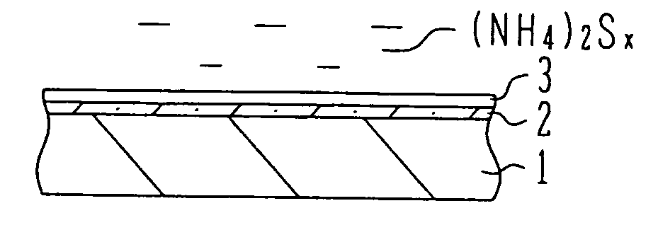
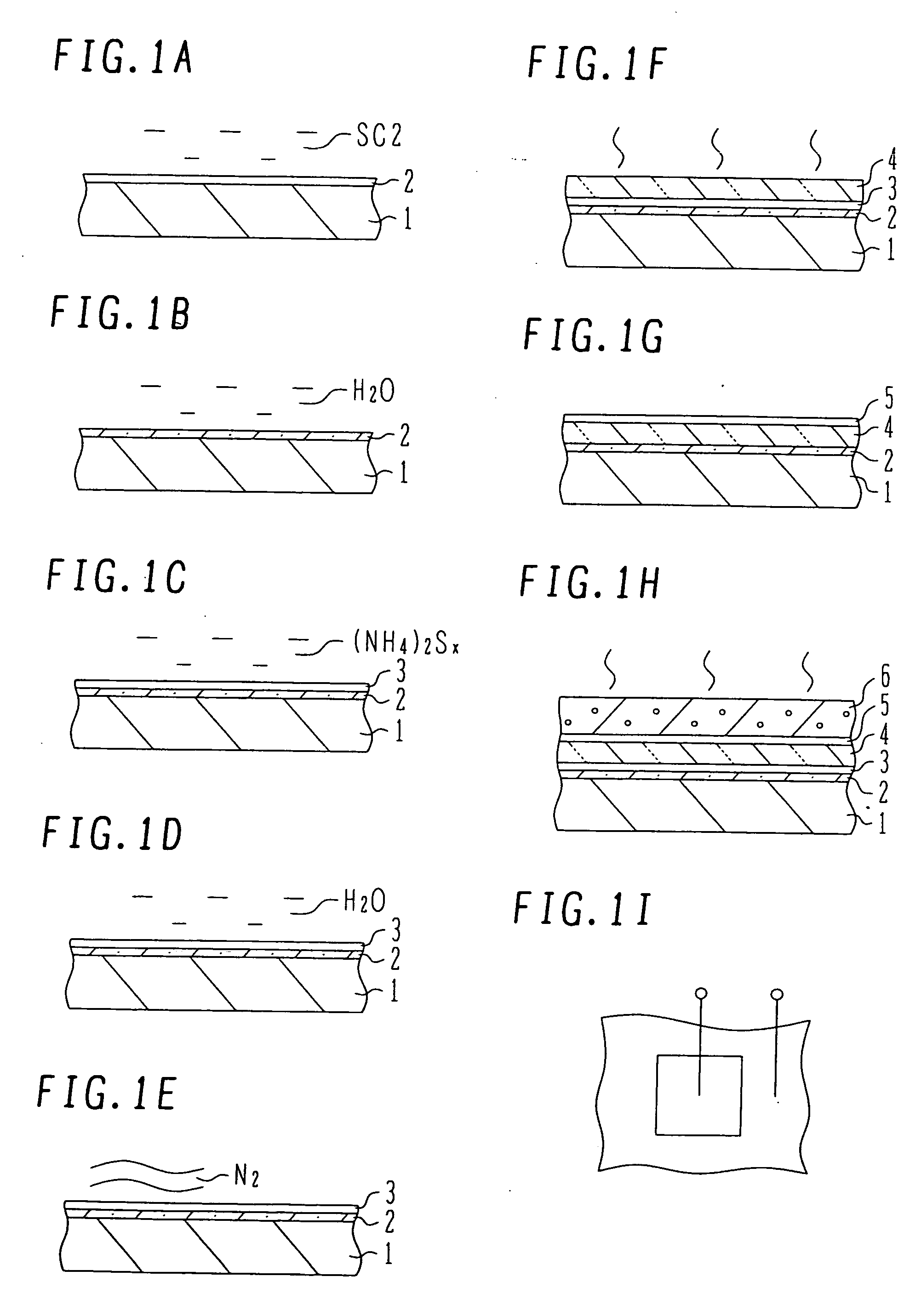
[0039] An SiO film or an SiON film is formed on the surface of the channel region of a MOS transistor in order to make the silicon substrate surface chemically and electrically stable. These films have a function of stabilizing the interface between the substrate and an upper layer and are called an interface layer.

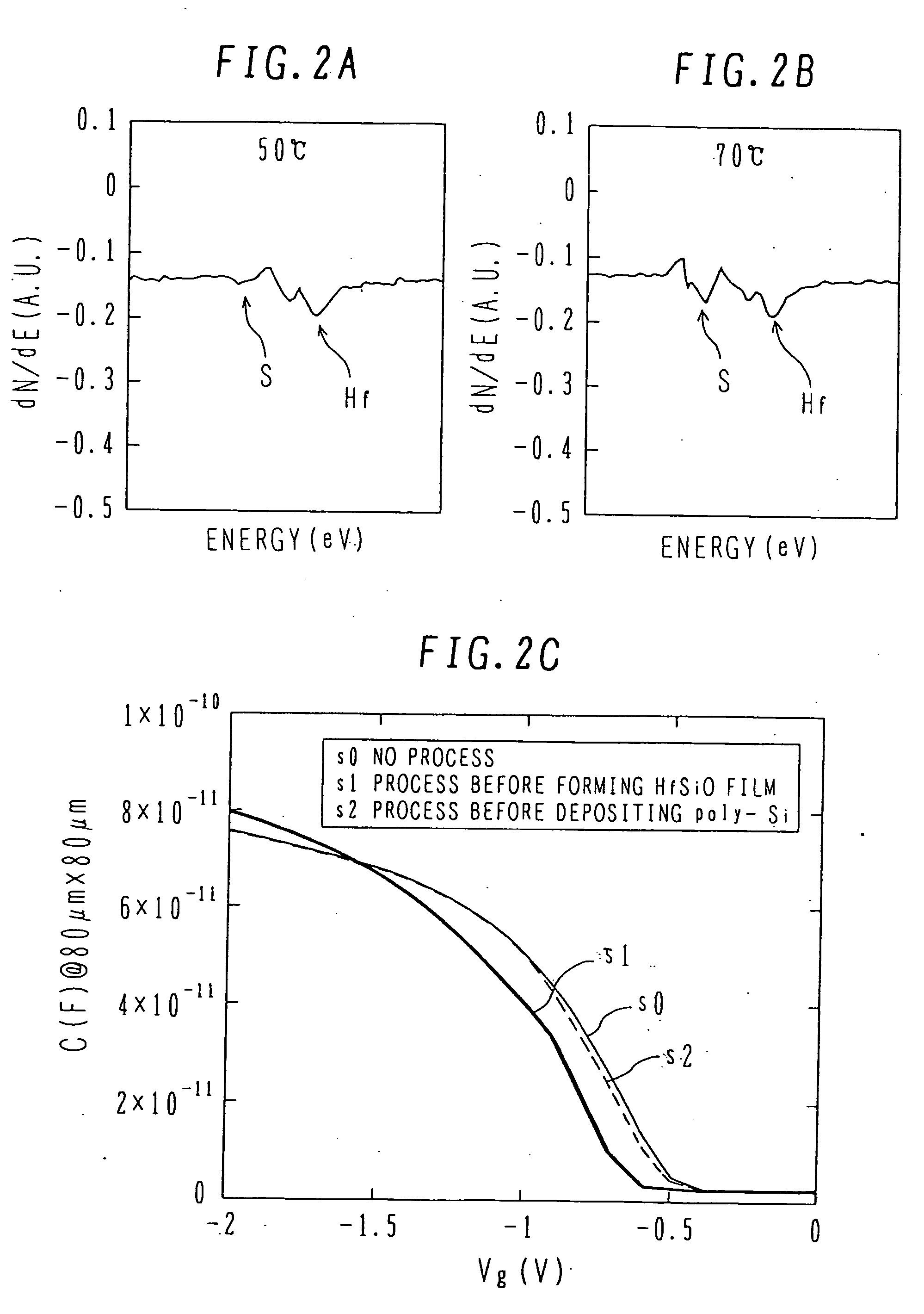
[0040] In the structure of polysilicon / high-k (HfO) insulating film / SiO(N) interface layer / silicon substrate, it has been found that an interface reaction, Hf—Si coupling and the like occur at the interface between the high-k insulating film and the SiO(N) interface layer and at the interface between polysilicon and the high-k insulating film. Because of these phenomena, it is very difficult to form an electrically good interface, and it has been observed that fixed charges are generated on the channel side and Fermi pinning (pinning Fermi level) phenomenon is induced on the gate electrode side. There are therefore adverse effects on the electric characteristics such as ...


PUM

PropertyMeasurementUnit
temperatureaaaaaaaaaa
gate lengthaaaaaaaaaa
thicknessaaaaaaaaaa

Abstract

A semiconductor device manufacture method has the steps of: (a) forming an interface layer of SiO or SiON on the surface of an active region of a silicon substrate; (b) forming a high dielectric constant gate insulating film such as HfSiON having a dielectric constant higher than that of silicon oxide, above the interface layer; (c) forming a gate electrode of polysilicon above the high dielectric constant gate insulating film; (d) passivating the substrate surface at least before or after the high dielectric constant gate insulating film is formed; (e) forming an insulated gate electrode structure by patterning at least the gate electrode and the high dielectric constant gate insulating film; and (f) forming source / drain regions in the active region on both sides of the insulated gate electrode structure. The semiconductor device has the high dielectric constant insulating film having a dielectric constant higher than that of silicon oxide.

Description

CROSS REFERENCE TO RELATED APPLICATION [0001] This application is based on and claims priority of Japanese Patent Application No. 2005-021029 filed on Jan. 28, 2005, the entire contents of which are incorporated herein by reference. BACKGROUND OF THE INVENTION [0002] A) Field of the Invention [0003] The present invention relates to a semiconductor device and its manufacture method, and more particularly to a semiconductor device having a high dielectric constant gate insulating film and its manufacture method. [0004] B) Description of the Related Art [0005] Insulated gate (IG) type field effect transistors (FET), typically MOS transistors, are widely used as representative semiconductor elements of a semiconductor integrated circuit device. In order to achieve high integration of semiconductor integrated circuit devices, IG-FETs have been miniaturized in accordance with scaling rules. Miniaturization such as thinning a gate insulating film and shortening a gate length reduces each s...

Claims


Application Information

Patent Timeline
Patent Type & Authority Applications(United States)
IPC IPC(8): H01L21/336H01L21/8238H01L21/8234H01L21/3205
CPCH01L21/28185H01L21/28194H01L21/823857H01L29/513H01L29/517
Inventor YAMAGUCHI, MASAOMIMINAKATA, HIROSHISAKODA, TSUNEHISAIKEDA, KAZUTO
Owner FUJITSU LTD
Why Eureka
Try Eureka