Non-synchronous boost converter including switched schottky diode for true disconnect

a boost converter and diode technology, applied in the direction of electric variable regulation, process and machine control, instruments, etc., can solve the problems of reducing battery life, affecting the efficiency of voltage converters at higher voltages, and unsatisfactory current flow through the diode to the output load

Active Publication Date: 2006-08-10
MICREL
View PDF11 Cites 142 Cited by
  • Summary
  • Abstract
  • Description
  • Claims
  • Application Information

AI Technical Summary

Benefits of technology

[0006] According to one embodiment of the present invention, a non-synchronous boost converter receiving an input DC voltage and providing an output DC voltage greater than the input DC voltage includes a controller, a switched Schottky diode, an inductor, a capacitor and a voltage divider. The controller is coupled to receive the input DC voltage on an input voltage terminal and generate a switched output voltage on a switched output voltage terminal. The controller further receives an enable signal on an enable terminal and a feedback voltage on a feedback terminal. The enable signal is asserted to turn on the boost converter and is deasserted to turn off the boost converter. The switched Schottky diode has an anode terminal coupled to the switched output voltage terminal, a cathode terminal providing the o

Problems solved by technology

When the boost converter is not being used, such as when the boost converter is disabled by deasserting the Enable signal, the DC current path remains which results in undesirable current flow through the Schottky diode to the output load.
Such leakage current is not desirable particularly when the boost converter is being used in a battery application where the leakage current can drain the battery, reducing the battery life.
But synchronous rectificatio

Method used


Image

  • Non-synchronous boost converter including switched schottky diode for true disconnect
  • Non-synchronous boost converter including switched schottky diode for true disconnect

Examples


Embodiment Construction

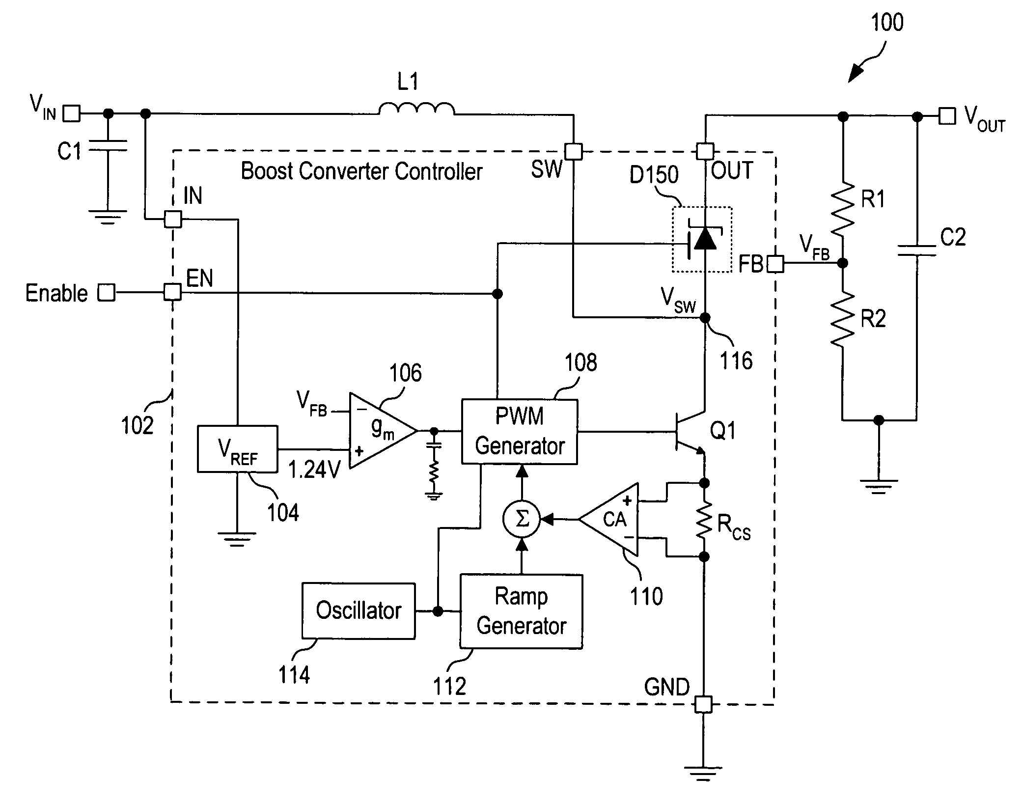
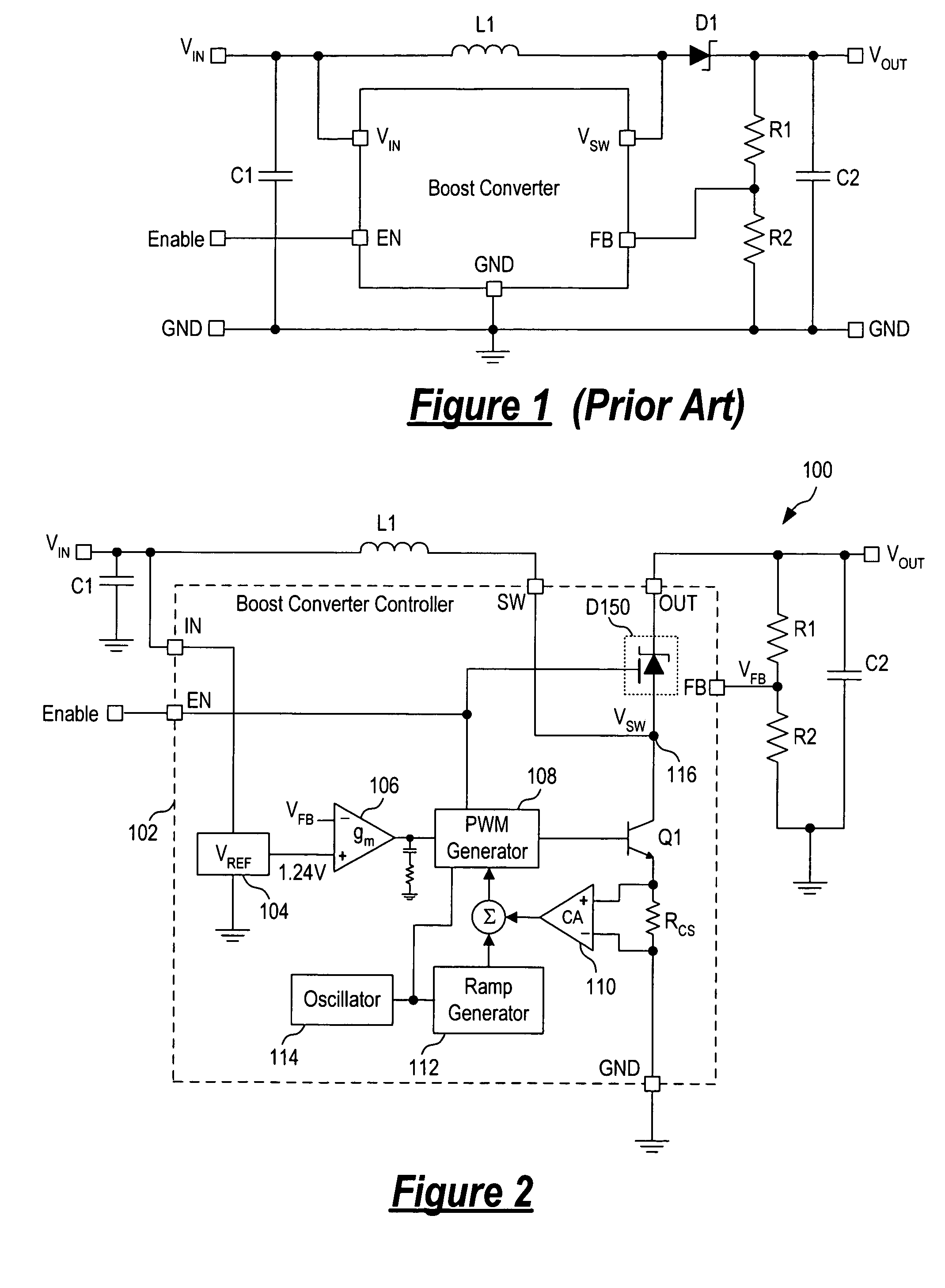
[0012] In accordance with the principles of the present invention, a boost converter includes a switched Schottky diode to rectify the switched output voltage of the boost converter where the switched Schottky diode has forward conduction blocking capability. Specifically, the switched Schottky diode has an anode terminal coupled to receive the switched output voltage and a cathode terminal providing the DC output voltage of the boost converter. The switched Schottky diode further includes a gate terminal coupled to receive a control signal for turning the switched Schottky diode on and off. When an enable signal coupled to the gate terminal is asserted to turn the switched Schottky diode on, the switched Schottky diode operates as a normal Schottky diode. When the enable signal coupled to the gate terminal is deasserted to turn the switched Schottky diode off, no forward current flows through the switched Schottky diode even when the anode terminal is forward biased relative to the...


PUM


Abstract

A non-synchronous boost converter includes a switched Schottky diode to rectify the switched output voltage of the boost converter where the switched Schottky diode has forward conduction blocking capability. The switched Schottky diode has an anode terminal coupled to receive the switched output voltage, a cathode terminal providing the output DC voltage, and a gate terminal coupled to receive a control signal. The control signal has a first state for turning the switched Schottky diode on where the switched Schottky diode conducts current when forward biased and a second state for turning the switched Schottky diode off where forward conduction of the switched Schottky diode is blocked even when the diode is forward biased. The switched Schottky diode can be a JFET controlled or an LDMOS gate controlled Schottky diode. Furthermore, the switched Schottky diode can be formed on-chip or off-chip of the controller circuit of the boost converter.

Description

CROSS-REFERENCE TO RELATED APPLICATIONS [0001] This application is related to the following commonly assigned U.S. patent applications: Ser. No. ______ (Attorney Docket No. MIC-M126), entitled “JFET Controlled Schottky Barrier Diode,” of Shekar Mallikarjunaswamy; and Ser. No. ______ (Attorney Docket No. M122), entitled “MOS gate controlled Schottky Diode,” of Shekar Mallikarjunaswamy. The aforementioned patent applications are incorporated herein by reference in their entireties.FIELD OF THE INVENTION [0002] The invention relates to voltage converters and, in particular, to a non-synchronous boost converter using a switched Schottky Diode to disconnect the switched output voltage from the output load. DESCRIPTION OF THE RELATED ART [0003] Step-up converters, or boost converters, are known in the art and operate by taking a DC input voltage and regulating a higher DC output voltage. FIG. 1 is a circuit diagram illustrating a typical circuit configuration of a conventional non-synchro...

Claims


Application Information

Patent Timeline
IPC IPC(8): G05F1/656G05F1/652
CPCH02M3/155H02M3/156H02M2001/0048H03K17/0826H03K17/74Y02B70/1491H02M1/0048Y02B70/10
Inventor MCGINTY, JOHNCOWELL, ANDREW
Owner MICREL
Why Eureka
Try Eureka