3-D transformer for high-frequency applications

Inactive Publication Date: 2006-08-10
PURDUE RES FOUND INC
View PDF25 Cites 2 Cited by
  • Summary
  • Abstract
  • Description
  • Claims
  • Application Information

AI Technical Summary

Benefits of technology

[0014] Finally, after the processing steps are complete, an electroplating process is performed to improve t

Problems solved by technology

With fT and fmax of the transistor approaching 200 GHz, the requirement for high performance passive elements is the bottleneck in designing state-of-the-art RF circuits.
Some of these approaches may use unconventional fabrication technologies that are difficult to integrate, such as the use of metals like Co.
Thicker metallization and

Method used


Image

  • 3-D transformer for high-frequency applications
  • 3-D transformer for high-frequency applications
  • 3-D transformer for high-frequency applications

Examples


Embodiment Construction

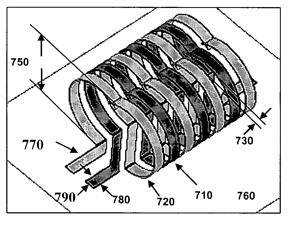
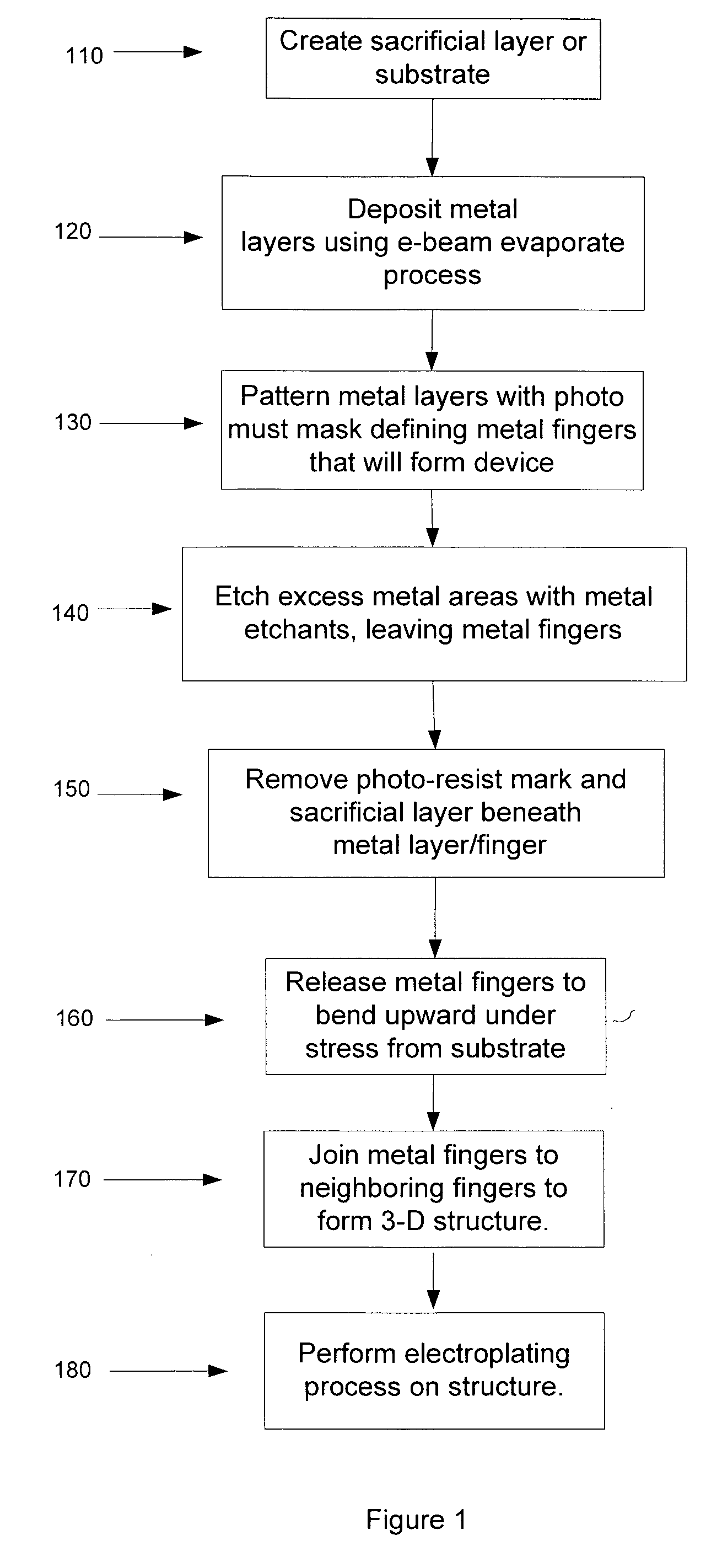
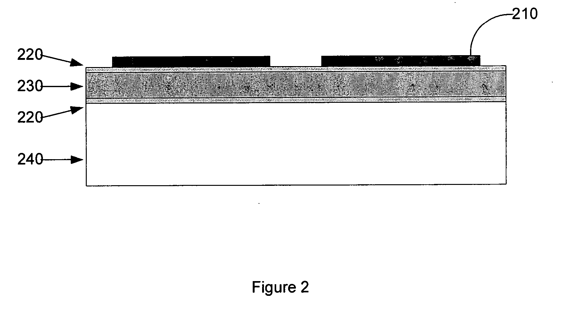
[0026]FIG. 1 presents a fabrication process for producing a high-Q, three-dimensional inductor or transformer. A sacrificial layer of photo-resist 210 (see FIG. 2) is deposited, at block 110, using semiconductor photolithographic processing equipment, on a pre-processed silicon substrate 240. This pre-processed substrate may comprise high resistivity silicon 240, silicon dioxide (SiO2) 220, or high dielectric constant materials such as SU-8™230. The photo-resist 210 may be a negative or positive-type photo-resist, as needed to operate with the photolithography process. The photo-resist 210 may be a polymer sensitive to certain wavelengths of light, typically ultraviolet radiation. A mask plate (not shown) that embodies an image of the structures to print on the circuit may be placed above the photo-resist layer 210 and the photo-resist is exposed to an ultraviolet light. The exposed resist may be developed in a solution. The solution may be a base such as potassium hydroxide (KOH). ...


PUM

PropertyMeasurementUnit
Electrical conductivityaaaaaaaaaa
Diameteraaaaaaaaaa
Structureaaaaaaaaaa

Abstract

A stressed metal technology may fabricate high-Q, three-dimensional microelectronic inductors and transformers. The fabrication method may allow the production of inductors and transformers on high-resistivity silicon substrate and with metal deposition of Au and Cr that is fully compatible with semiconductor fabrication technologies. The produced inductors and transformers exhibit Q factors>60 at frequencies of 3 to 7 GHz. High efficiency, high-Q transformers with coupling factors 0.6<k<0.9 may be created with very high self-resonance frequencies

Description

PRIORITY CLAIM [0001] This application claims the benefit of priority from U.S. Provisional Application No. 60 / 634,713, filed Dec. 8, 2004, which is incorporated herein by reference.BACKGROUND [0002] 1. Technical Field [0003] This invention relates to semiconductor processing of electronic components. In particular, the invention relates to 3-D inductor and transformer elements formed by semiconductor processing. [0004] 2. Related Art [0005] Nanoscale CMOS and SiGe BiCMOS processes have recently enhanced the performance of Si-based RFICs up to microwave frequencies. With fT and fmax of the transistor approaching 200 GHz, the requirement for high performance passive elements is the bottleneck in designing state-of-the-art RF circuits. Inductors and transformers play a role in the performance achieved by RF circuits such as voltage controlled oscillators (VCOs), low-noise amplifiers (LNAs), filters, mixers, and power amplifiers (PAs). Among inductor and transformer parameters that lim...

Claims


Application Information

Patent Timeline
IPC IPC(8): H01F5/00
CPCH01F17/0033Y10T29/4902H01F41/041H01F17/02H01F17/0006B33Y10/00H01F5/00
Inventor WEON, DAE-HEEMOHAMMADI, SAEEDJEON, JONG-HYEOKKATEHI, LINDA P.B.
Owner PURDUE RES FOUND INC
Why Eureka
Try Eureka