Preparation of metal silicon nitride films via cyclic deposition

a metal silicon nitride and cyclic deposition technology, applied in the field of metal silicon nitride films via cyclic deposition, can solve the problems of difficult to achieve the barrier performance of copper diffusion, affecting the performance of devices, and affecting the stability of films, etc., and achieve the effect of increasing film stability

Inactive Publication Date: 2006-08-17
VERSUM MATERIALS US LLC
View PDF21 Cites 345 Cited by
  • Summary
  • Abstract
  • Description
  • Claims
  • Application Information

AI Technical Summary

Benefits of technology

[0020] an ability to produce high quality ternary metal silicon nitride films;
[0021] an ability to form high quality films while eliminating some of the common precursors that present significant safety and corrosion issues; and,
[0024] an ability to achieve excellent deposition rates in a cyclic CVD, thus making possible an increase of wafer throughput at production scale;
[0026] an ability to produce metal silicon nitride films using two precursors while eliminating the use of a separate nitrogen source, e.g., ammonia;
[0027] an ability to reduce the metal center in a resulting metal silicon, thus reducing the resisitivity of the resulting film; and,
[0028] an ability to increase the film stability by forming metal-nitrogen-silicon linkages in the resulting metal silicon nitride.

Problems solved by technology

Electromigration of copper into the silicon substrate ruins device performance.
Barrier performance to copper diffusion as, for example, has been difficult to achieve.
Currently in the formation of ternary films, a metal amide, silane, and ammonia are sequentially deposited on the substrate via cyclic deposition but the process poses processing issues.
Silane is a pyrophoric gas and creates a potential safety hazard.

Method used


Image

  • Preparation of metal silicon nitride films via cyclic deposition
  • Preparation of metal silicon nitride films via cyclic deposition
  • Preparation of metal silicon nitride films via cyclic deposition

Examples


example 1

Deposition of TiSiN Films from TDMAT and BTBAS at 200° C.

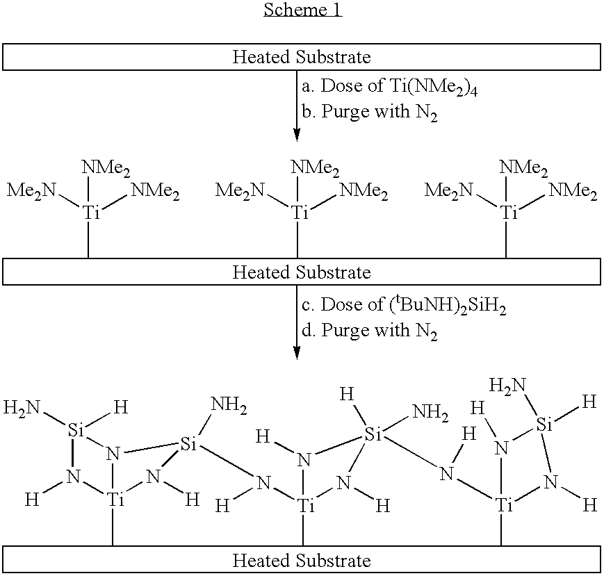
[0062] A silicon wafer is charged to a deposition chamber and maintained at a temperature of 200° C. and a pressure of 200 Pa (1.5 Torr). A Ti-containing compound of 2.6 micromoles, tetrakis(dimethylamino)titanium (TDMAT), is introduced into the chamber over a period of 10 seconds pulse along with 100 sccm N2. After deposition of the Ti amide, the unreacted Ti amide and byproducts are purged with 2000 sccm N2 for 7.5 seconds. Then, a dose 4.73 micromoles of a Si-containing compound, bis(tert-butylamino)silane (BTBAS), is introduced over a period of 80 seconds along with 100 sccm N2. Unreacted BTBAS and byproduct are removed by a 40 second purge with 2000 sccm of N2.

[0063] The above cycle is repeated for 200 cycles (of the 4 steps) and a film of 45 Å thickness is generated. The deposition rate per cycle is 0.22 Å which is much lower than a typical ALD process, showing this temperature is insufficient for these precursors to a...

example 2

ALD Formation of TiSiN Films from TDMAT and BTBAS at 250° C.

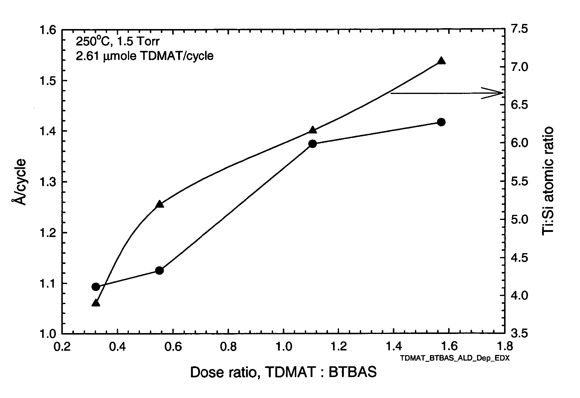
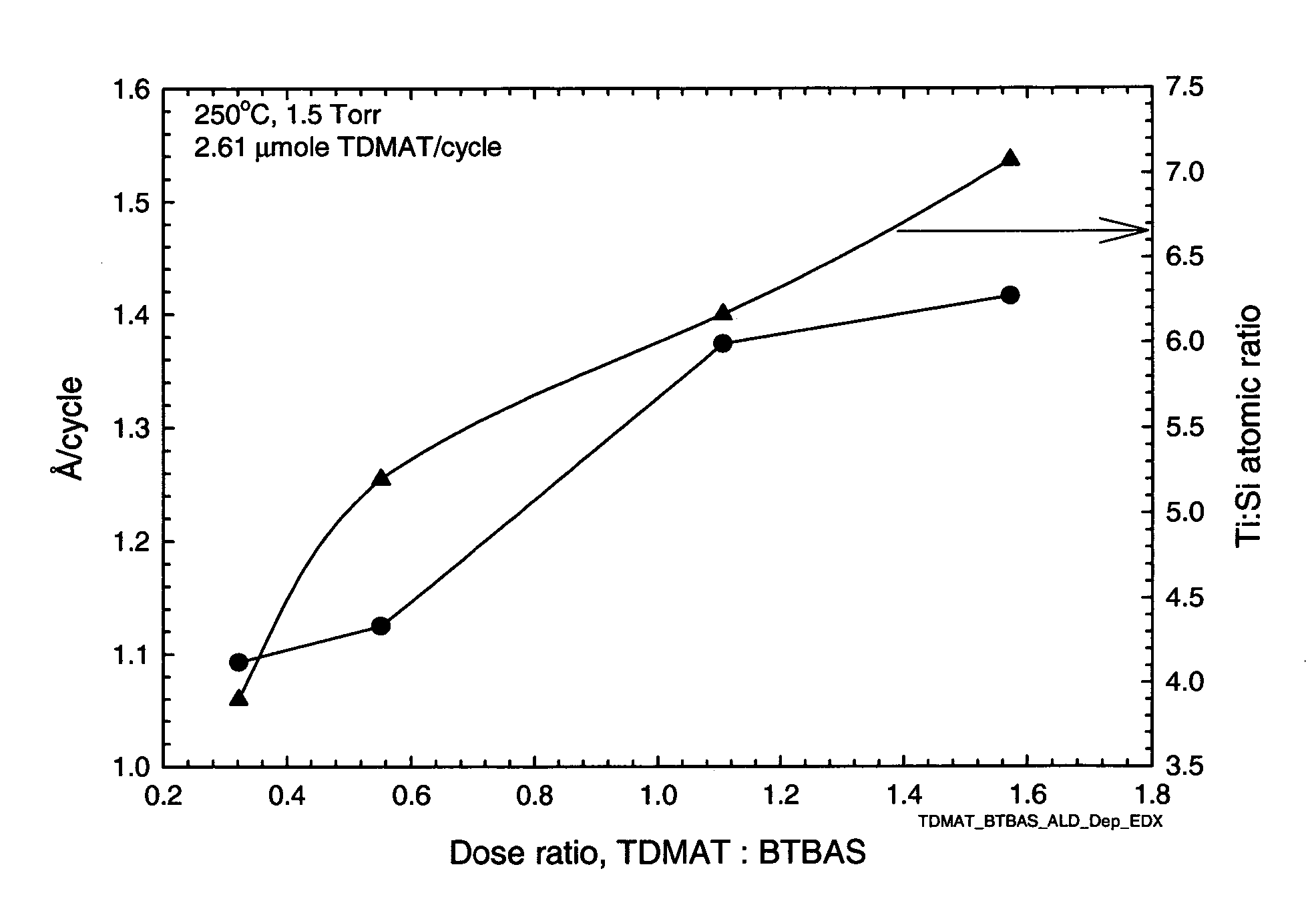
[0064] The procedure of Example 1 is followed except that the silicon wafer is maintained at a temperature of 250° C. and a pressure of 200 Pa (1.5 Torr). A Ti-containing compound of 2.6 micromoles, tetrakis(dimethylamino)titanium (TDMAT) is introduced for 10 seconds into the chamber with 100 sccm N2. A purge of 2000 sccm N2 follows for 7.5 seconds. Then a dose 4.73 micromoles of a Si-containing compound, bis(tert-butylamino)silane (BTBAS), is introduced for 80 seconds along with 100 sccm N2. This is followed by a 40 second purge with 2000 sccm of N2. The cycle was repeated for 100 cycles (of the 4 steps) and a film of 144 Å thickness was generated.

[0065] The deposition rate per cycle is 1.44 Å which falls in the range for a typical ALD process, showing this temperature is sufficient to achieve monolayer surface saturation. The Ti to Si molar input ratio is 0.55 and the Ti to Si atomic ratio in the deposited film is analy...

example 3

Cyclic CVD Formation of TiSiN Films from TDMAT and BTBAS

[0067] The procedure of Example 1 is followed except the silicon wafer is maintained at a temperature of 300° C. and a pressure of 200 Pa (1.5 Torr). A Ti-containing compound of 2.6 micromoles, tetrakis(dimethylamino)titanium (TDMAT), is introduced for 10 seconds into the chamber with 100 sccm N2. A purge of 2000 sccm N2 follows for 7.5 seconds. Then a dose 4.73 micromoles of a Si-containing compound, bis(tert-butylamino)silane(BTBAS), is introduced for 80 seconds along with 100 sccm N2. This is followed by a 40 second purge with 2000 sccm of N2. This is repeated for 100 cycles (of the 4 steps) and produces a film of 629 Å thickness. The rate per cycle is 6.29 Å, showing this temperature is too high to limit deposition to a monolayer per cycle. In contrast to Examples 1 and 2, a cyclic CVD-like process occurred at this temperature, leading to a deposition rate much higher than in an ALD process.

[0068] The Ti to Si molar input...


PUM

PropertyMeasurementUnit
temperatureaaaaaaaaaa
pressureaaaaaaaaaa
temperatureaaaaaaaaaa

Abstract

This invention relates to an improved process for producing ternary metal silicon nitride films by the cyclic deposition of the precursors. The improvement resides in the use of a metal amide and a silicon source having both NH and SiH functionality as the precursors leading to the formation of such metal-SiN films. The precursors are applied sequentially via cyclic deposition onto the surface of a substrate. Exemplary silicon sources are monoalkylamino silanes and hydrazinosilanes represented by the formulas: (R1NH)nSiR2mH4-n-m (n=1,2; m=0,1,2; n+m=<3); and (R32N—NH)xSiR4yH4-x-y (x=1,2; y=0,1,2; x+y=<3) wherein in the above formula R1-4 are same or different and independently selected from the group consisting of alkyl, vinyl, allyl, phenyl, cyclic alkyl, fluoroalkyl, silylalkyls.

Description

BACKGROUND OF THE INVENTION [0001] Metal silicon nitride films are known and have been used in the semiconductor industry to provide a diffusion barrier for interconnects and they have been used as gate electrodes. Traditionally, aluminum has been used for interconnects in semiconductor devices, but recently, copper, with its lower resistance and better electromigration lifetime than that of aluminum, has been used for integration. However, copper is very mobile in many of the materials used to fabricate semiconductor devices and can diffuse quickly through certain materials including dielectrics. Electromigration of copper into the silicon substrate ruins device performance. Thus, it is necessary to have barrier layers in place to avoid any diffusion within the semiconductor device. [0002] Metal nitride layers, e.g., titanium nitride (TiN) layers have been employed as barrier layers against diffusion, including copper diffusion, in semiconductor device structures, e.g., contacts, v...

Claims


Application Information

Patent Timeline
Patent Type & Authority Applications(United States)
IPC IPC(8): C23C16/00
CPCC23C16/34C23C16/345C23C16/45531C23C16/45553H01L21/28562H01L21/28568H01L21/318H01L21/02205H01L21/02219H01L21/02142H01L21/02216H01L21/0228H01L21/0215H01L21/02153A47G33/00F21V21/06A47G2200/08H01L21/0234
Inventor LEI, XINJIANTHRIDANDAM, HAREESHCUTHILL, KIRK SCOTTHOCHBERG, ARTHUR KENNETH
Owner VERSUM MATERIALS US LLC
Why Eureka
Try Eureka