
Semiconductor device and method for producing the same

a technology of semiconductor devices and semiconductors, applied in semiconductor devices, semiconductor/solid-state device details, electrical apparatus, etc., can solve the problems of voids, interconnect breakdowns, and voids, so as to detract from the characteristics of devices, and the diffusion of copper (cu) atoms into silicon (si) substrates or insulating films,

Inactive Publication Date: 2006-08-17
RENESAS ELECTRONICS CORP
View PDF7 Cites 0 Cited by
  • Summary
  • Abstract
  • Description
  • Claims
  • Application Information

AI Technical Summary

Benefits of technology

The use of materials with closely matched unit cell dimensions significantly reduces copper diffusion, enhancing electromigration resistance and preventing voids and interconnect failures in semiconductor devices.

Problems solved by technology

However, diffusion of copper (Cu) atoms into silicon (Si) substrates or insulating films will detract from the characteristics of the devices.
The problem with the devices is so-called electromigration.
However, layered interconnect structures in which a diffusion barrier of, for example, a titanium nitride (TiN) film, a tungsten (W) film or a tantalum (Ta) film is kept in contact with a copper (Cu) film could not have satisfactory electromigration resistance, and therefore often pose the problem of voids and interconnect breakdowns.

Method used


Image

  • Semiconductor device and method for producing the same
  • Semiconductor device and method for producing the same
  • Semiconductor device and method for producing the same

Examples


first embodiment

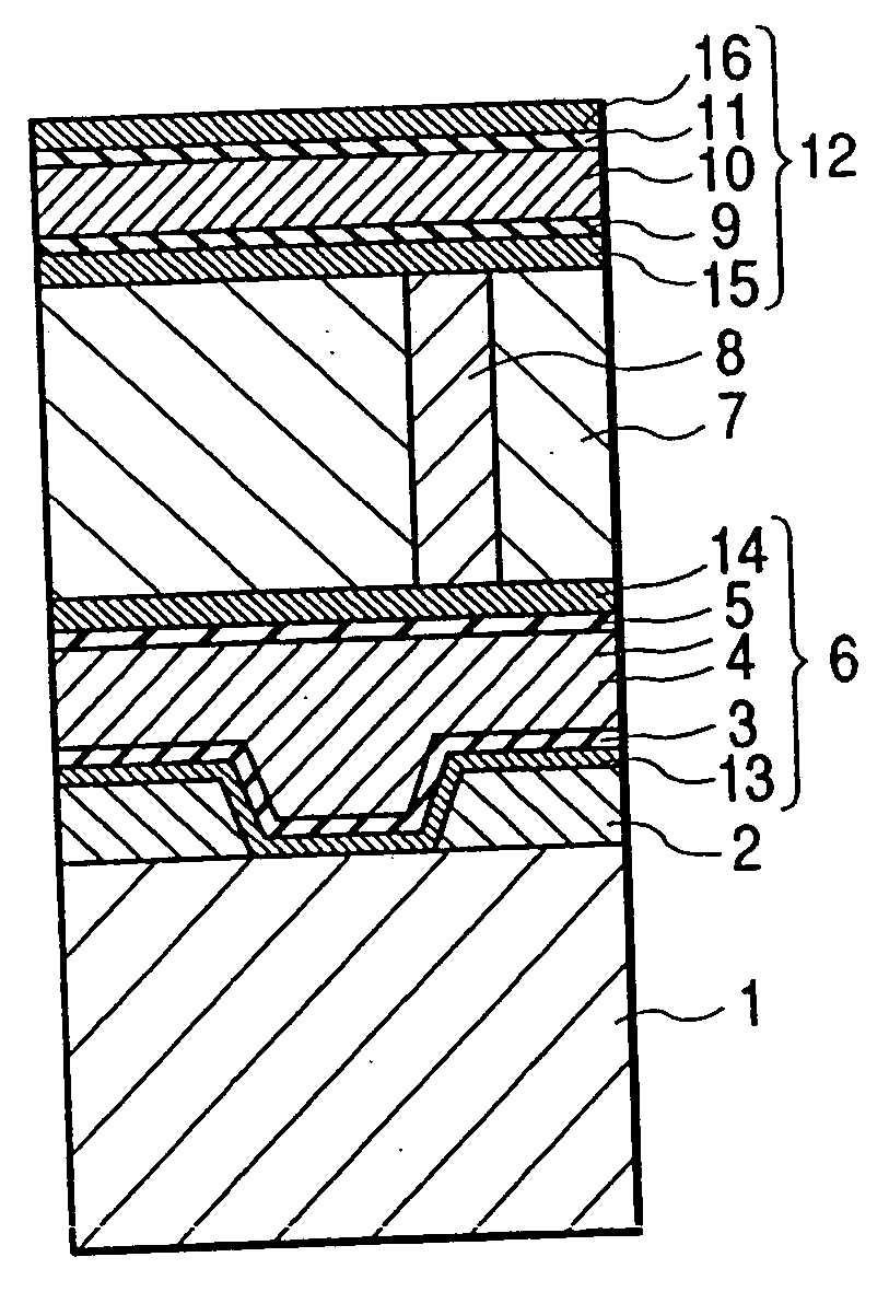
[0032] First referred to is FIG. 1, which shows a cross-sectional structure of the layered interconnect structure part of a semiconductor device of the invention.

[0033] As in FIG. 1, the layered interconnect structure in the semiconductor device of this embodiment comprises an insulating film 2 of, for example, silicon oxide as formed on a silicon substrate 1, in which a first layered interconnect structure 6 composed of a neighboring film 3, a conductor film 4 and a neighboring film 5 is connected with the substrate 1 via a contact hole as formed through the insulating film 2. In this, an insulating film 7 of, for example, silicon oxide is formed on the first layered interconnect structure 6, and a via 8 of, for example, tungsten (W) is filled in the via hole as formed through the insulating film 7. Through this via 8, a second layered interconnect structure 12 composed of a neighboring film 9, a conductor film 10 and a neighboring film 11 is connected with the first layered interc...

second embodiment

[0039] Next referred to is FIG. 7 which shows a cross-sectional structure of a layered interconnect structure part of a semiconductor device of the invention.

[0040] As in FIG. 7, the layered interconnect structure in the semiconductor device of this embodiment comprises an insulating film 2 of, for example, silicon oxide as formed on a silicon substrate 1, in which a first layered interconnect structure 6 composed of a diffusion barrier 13, a neighboring film 3, a conductor film 4, a neighboring film 5 and a diffusion barrier 14 is connected with the substrate 1 via a contact hole as formed through the insulating film 2. In this, an insulating film 7 of, for example, silicon oxide is formed on the first layered interconnect structure 6, and a via 8 of, for example, tungsten (W) is filled in the via hole as formed through the insulating film 7. Through this via 8, a second layered interconnect structure 12 composed of a diffusion barrier 15, a neighboring film 9, a conductor film 10,...

third embodiment

[0042] Next referred to is FIG. 8 which shows a cross-sectional structure of a principal part of a semiconductor device of the invention. As in FIG. 8, the semiconductor device of this embodiment comprises diffusion layers 102, 103, 104, 105 all formed on a silicon substrate 101, on which are formed gate-insulating films 106, 107 and gate electrodes 108, 109 to construct MOS transistors. The gate-insulating films 106, 107 are, for example, silicon oxide films or silicon nitride films; and the gate electrodes 108, 109 are, for example, polycrystalline silicon films, thin metal films or metal silicide films, or are of a layered structure comprising any of them. The MOS transistors are separated from each other by an isolation film 110 of, for example, a silicon oxide film. The gate electrodes 108, 109 are covered with insulating films 111, 112, respectively, of, for example, silicon oxide films, entirely on their top and side surfaces. The MOS transistors are entirely covered with an ...


PUM


Abstract

Provided is a reliable semiconductor device with a layered interconnect structure that may develop no trouble of voids and interconnect breakdowns, in which the layered interconnect structure comprises a conductor film and a neighboring film as so layered on a semiconductor substrate that the neighboring film is contacted with the conductor film. In the device, the materials for the conductor film and the neighboring film are so selected that the difference between the short side, ap, of the rectangular unit cells that constitute the plane with minimum free energy of the conductor film and the short side, an, of the rectangular unit cells that constitute the plane with minimum free energy of the neighboring film, {|ap-an| / ap}x100=A (%) and the difference between the long side, bp, of the rectangular unit cells that constitute the plane with minimum free energy of the conductor film and the long side, bn, of the rectangular unit cells that constitute the plane with minimum free energy of the neighboring film, {|bp-bn| / bp}x100=B (%) satisfy an inequality of {A+Bx(ap / bp)}<13. In this, the diffusion of the conductor film is retarded.

Description

[0001] This application is a Continuation application of application Ser. No. 10 / 878,018, filed Jun. 29, 2004, which is a Continuation application of application Ser. No. 09 / 985,904, filed Nov. 6, 2001, which is a Continuation application of application Ser. No. 09 / 255,856, filed Feb. 23, 1999, the contents of which are incorporated herein by reference in their entirety.BACKGROUND OF THE INVENTION [0002] The present invention relates to a semiconductor device, in particular, to that with a layered interconnect structure. [0003] In recent large-scale-integration, high-performance semiconductor devices, copper (Cu) interconnects are being employed as having lower electric resistance than conventional aluminum (Al) interconnects. However, diffusion of copper (Cu) atoms into silicon (Si) substrates or insulating films will detract from the characteristics of the devices. To prevent the copper (Cu) diffusion, a diffusion barrier is formed adjacent, to the copper (Cu) film. As the materia...

Claims


Application Information

Patent Timeline
Patent Type & Authority Applications(United States)
IPC IPC(8): H01L21/44H01L23/532
CPCH01L21/76846H01L21/76849H01L21/7685H01L23/53228H01L23/53238H01L2924/0002H01L23/53252H01L2221/1078H01L23/53242H01L2924/00H01L21/28
Inventor IWASAKI, TOMIOMIURA, HIDEO
Owner RENESAS ELECTRONICS CORP
Learn More