High pressure treatment for improved grain growth and void reduction

a high-pressure treatment and grain technology, applied in semiconductor/solid-state device manufacturing, basic electric elements, electric devices, etc., can solve the problems of reduced resistivity, physical change of copper structure, and shrinkage of copper lines, so as to improve grain growth and reduce micro-voids , the effect of increasing the temperature in the process chamber

Inactive Publication Date: 2006-08-17
WAFERMASTERS
View PDF3 Cites 8 Cited by
  • Summary
  • Abstract
  • Description
  • Claims
  • Application Information

AI Technical Summary

Benefits of technology

[0010] According to one aspect of the present invention, a copper film anneal is performed at pressures higher than atmospheric to enhance grain growth and reduce micro-voids. Pressure greater than 1 atmosphere, for example, up to 500 atmospheres, applied to a porous material, such as copper, forces micro-voids to escape to the surface. The pressure can be applied to a semiconductor device inside a process chamber, the device having a copper film, other metal film, dielectric film, or other suitable semiconductor film formed thereon, such as a copper film formed by a dual damascene technique. High pressure liquid or gas can be introduced into the process chamber to raise the pressure to a suitable level.
[0011] In another embodiment, the temperature in the process chamber can be increased, along with the pressure. Increasing both the pressure and temperature enhances grain growth and aids in void removal. Since high pressure promotes grain growth and removes voids, a copper anneal or other similar process can operate at temperatures less than conventional temperatures. This enables process engineers to select a lower processing temperature while still producing a film that meets conventional standards. Thus, grain growth is possible at temperatures less than room temperature.

Problems solved by technology

However, as devices get smaller and smaller, the copper lines become increasingly thinner and narrower.
This results in a reduction in resistivity and a physical change in the copper structure.
However, copper self-anneal does not grow larger grains.
The adverse effects include a higher resistance in the lines with very small dimension due to electron scattering from grain boundaries, defects, and surfaces.
This method may be suitable for annealing blanket copper film, but with thin narrow copper wires (e.g., 500 or 1000 angstroms wide), annealing at higher temperatures can become problematic since the grain size approaches the size of the copper wire.
Growing grains in small wires is also difficult due to the amount of material available for the grain growth.
Grain growth also results in small micro-voids between the grains.
During anneal process steps, grain growth of the copper films also creates stresses that can damage or destroy the thin film.
The stresses lead to warping and bowing and ultimately to film cracking which undermines desired low resistivity of the copper.
Micro-voids can cause reliability problems and other associated adverse effects with the resulting copper film.
Self-annealing does not remove the micro-voids.

Method used


Image

  • High pressure treatment for improved grain growth and void reduction
  • High pressure treatment for improved grain growth and void reduction
  • High pressure treatment for improved grain growth and void reduction

Examples


Embodiment Construction

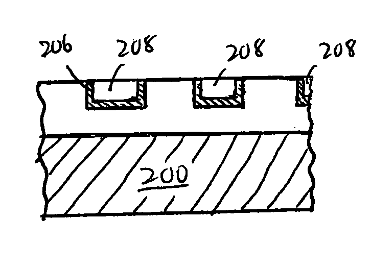
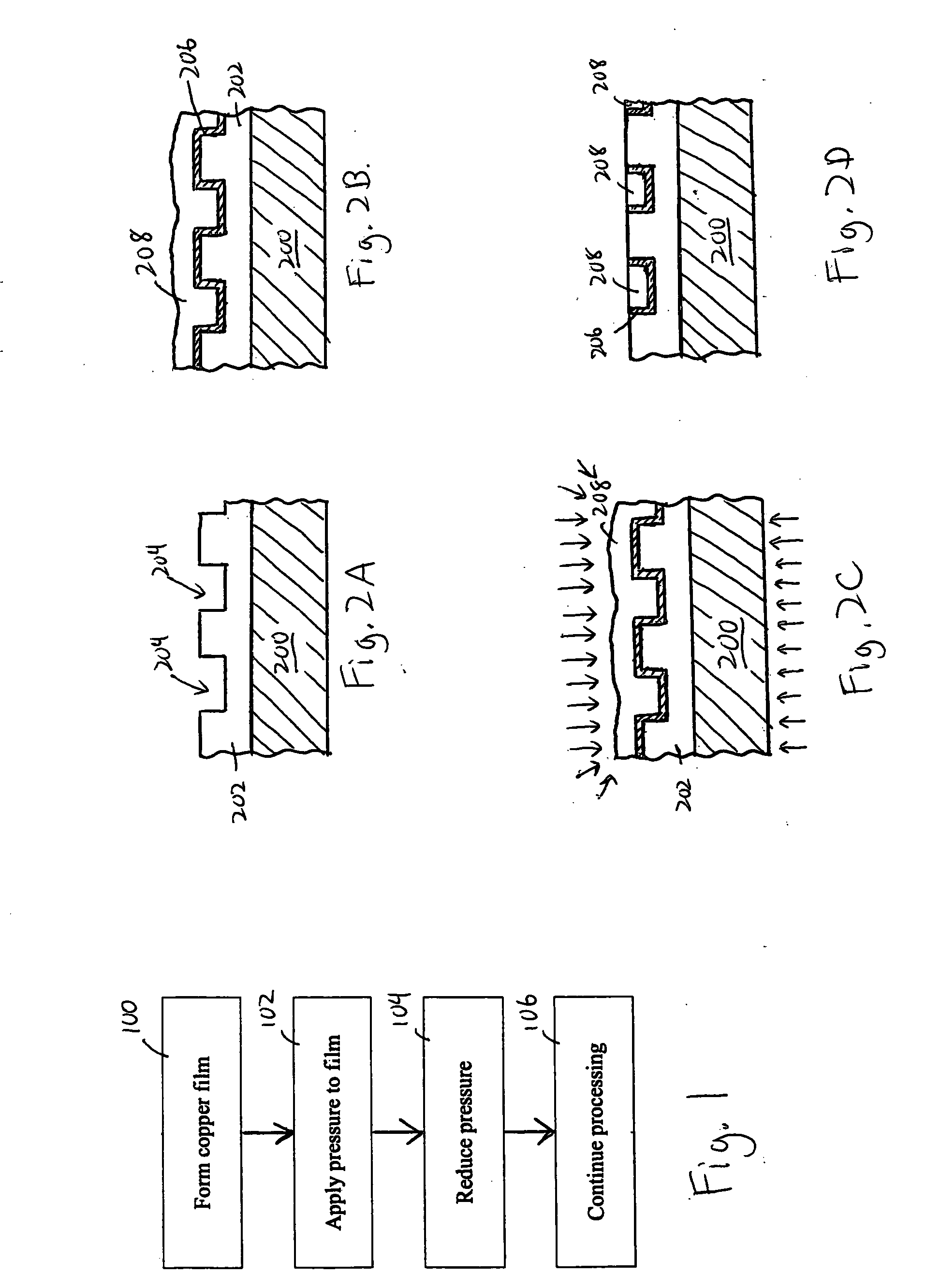
[0018]FIG. 1 is a flow chart showing one embodiment of the present invention for forming a copper layer on a semiconductor device during semiconductor processing. In step 100, a copper layer or film is formed on a semiconductor device in a high pressure process chamber. The copper film can be formed by any suitable conventional method, such as a dual damascene technique. In the dual damascene approach, a dielectric or insulating diffusion barrier layer is deposited over a copper layer. The dielectric layer is then patterned, e.g., by conventional masking and etching techniques, to form a two-step connection having a narrower lower portion (or via portion) exposing desired connection areas on the underlying patterned metal layer and a wider upper portion (or trench portion) that will form the next layer of metal lines. Copper is then deposited to fill the via and trench, such as by electroplating. The chamber is pressurized, in step 102, such as up to 500 atm. Chamber pressurization ...


PUM

PropertyMeasurementUnit
pressureaaaaaaaaaa
temperatureaaaaaaaaaa
pressureaaaaaaaaaa

Abstract

A copper film is annealed at high pressure to enhance grain growth and remove voids. Other films, such as dielectrics, may also be suitable. High pressure can be used in conjunction with temperatures lower than room temperature for annealing or higher temperatures may be used to further enhance grain growth.

Description

BACKGROUND OF THE INVENTION [0001] 1. Field of the Invention [0002] The present invention relates the manufacture of semiconductor devices, and more particular, to improving grain growth and reducing voids during such manufacturing. [0003] 2. Related Art [0004] Integrated circuits fabricated on semiconductor substrates for very and ultra large scale integration typically require multiple levels of metal layers to electrically interconnect the discrete layers of semiconductor devices on the semiconductor chips. The different levels of metal layers are separated by various insulating or dielectric layers (also known as interlevel dielectric (ILD) layers), which have etched via holes to connect devices or active regions from one layer of metal to the next. [0005] As semiconductor technology advances, circuit elements and dimensions on wafers or silicon substrates are becoming increasingly more dense. Consequently, the interconnections between various circuit elements and dielectric lay...

Claims


Application Information

Patent Timeline
Patent Type & Authority Applications(United States)
IPC IPC(8): H01L21/44
CPCH01L21/76882
Inventor YOO, WOO SIKKANG, KITAEK
Owner WAFERMASTERS
Why Eureka
Try Eureka