
Eureka
For R&D, Eureka makes reading and utilizing patents & technical documents easy.
Eureka AIR
Designed for self-driven R&D workflows. Generate viable solutions, solve complex R&D challenges, empower your innovation with AI.

Eureka Materials
Designed for material experts only. Revolutionize your material R&D, from search, analyze, to developing new materials.

TechResearch
Generate reliable direction feasibility study reports for your R&D in just a few steps.

TechSeek
Discover and master advanced knowledge NOW. Basics, ideas, possibilities, all at once.

TechMind
As an expert in R&D Theories, TechMind can generates customized viable solutions instantly.

TechRisk
Analyze your overall solution with one click, know your potential R&D risks in advance.

TechMonitor
Get weekly tech updates, stay abreast of the latest tech innovations and key insights.
Method of forming silicon-containing insulation film having low dielectric constant and low diffusion coefficient
- Summary
- Abstract
- Description
- Claims
- Application Information
AI Technical Summary
Benefits of technology
Problems solved by technology
Method used
Image

Examples
example 1
[0078] Using the plasma CVD apparatus 1 shown in FIG. 1, an example of forming an insulation film on a Ø300 mm silicon substrate was performed.
[0079] Experimental conditions:
[0080] Primary gas: DM-DMOS (dimethyl-dimethoxysilane) 180 sccm
[0081] Additive gas: He 150 sccm
[0082] Secondary gas: Isopropyl alcohol 400 sccm
[0083] Oxygen-supplying gas: O2 0-80 sccm
[0084] 1st radio-frequency power source: 27.12 MHz 1.9 W / cm2
[0085] 2nd radio-frequency power source: 400 kHz 0 W / cm2
[0086] Pressure: 800 Pa
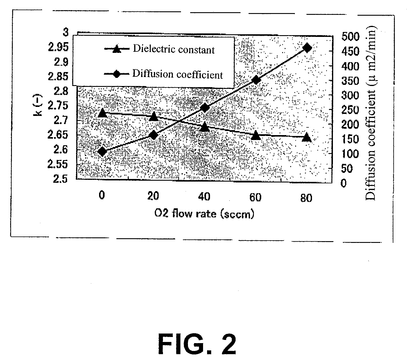
[0087]FIG. 2 is a graph showing the relationship between the dielectric constants and the diffusion resistance function when a flow rate of O2 was altered from 0 to 80 sccm under the above-mentioned experimental conditions. The graph demonstrates that under the above-mentioned experimental conditions, an optimized flow rate of O2 for forming an insulation film having a dielectric constant of 2.9 or lower and a diffusion coefficient of 250 μm2 / min or less is 0 to 40 sccm.
example 2
[0088] Using the plasma CVD apparatus shown in FIG. 1, an example of forming an insulation film on a Ø300 mm silicon substrate was performed.
[0089] Experimental conditions:
[0090] Primary gas: DM-DMOS (dimethyl-dimethoxysilane) 180 sccm
[0091] Additive gas: He 150 sccm
[0092] Secondary gas: Isopropyl alcohol 400 sccm
[0093] Oxygen-supplying gas: O2 0-80 sccm
[0094] 1st radio-frequency power source: 27.12 MHz 1.9 W / cm2
[0095] 2nd radio-frequency power source: 400 kHz 0.1 W / cm2
[0096] Pressure: 800 Pa
[0097]FIG. 3 is a graph showing the relationship between the dielectric constants and the diffusion blocking function when a flow rate of O2 was altered from 0 to 80 sccm under the above-mentioned experimental conditions. The graph demonstrates that under the above-mentioned experimental conditions, an optimized flow rate of O2 for forming an insulation film having a dielectric constant of 2.9 or lower and a diffusion coefficient of 250 μm2 or less is 0 to 40 sccm.
example 3
[0098] Using the plasma CVD apparatus shown in FIG. 1, an example of forming an insulation film on a Ø300 mm silicon substrate was performed.
[0099] Experimental conditions:
[0100] Primary gas: DMOTMDS (1,3-dimethoxytetramethyldisiloxane) 100 sccm
[0101] Additive gas: He 160 sccm
[0102] Secondary gas: Isopropyl alcohol 400 sccm
[0103] Oxygen-supplying gas: O2 0-75 sccm
[0104] 1st radio-frequency power source: 27.12 MHz 1.8 W / cm2
[0105] 2nd radio-frequency power source: 400 kHz 0 W / cm2
[0106] Pressure: 850 Pa
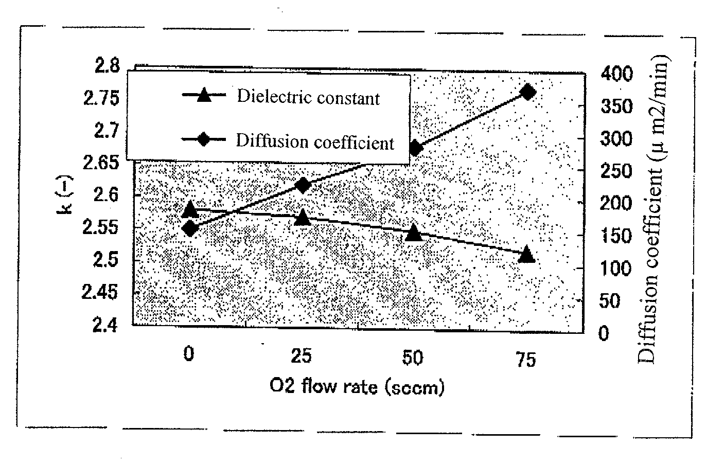
[0107]FIG. 4 is a graph showing the relationship between the dielectric constants and the diffusion blocking function when a flow rate of O2 was altered from 0 to 75 W / cm2 under the above-mentioned experimental conditions. The graph demonstrates that under the above-mentioned experimental conditions, an optimized flow rate of O2 for forming an insulation film having a dielectric constant of 2.7 or lower and a diffusion coefficient of 250 μm2 or less is 0 to 25 sccm.
PUM
| Property | Measurement | Unit |
|---|---|---|
| Temperature | aaaaa | aaaaa |
| Fraction | aaaaa | aaaaa |
| Fraction | aaaaa | aaaaa |
Abstract
Description
Claims
Application Information
 - R&D Engineer
- R&D Manager
- IP Professional
- Industry Leading Data Capabilities
- Powerful AI technology
- Patent DNA Extraction
Browse by: Latest US Patents, China's latest patents, Technical Efficacy Thesaurus, Application Domain, Technology Topic, Popular Technical Reports.
© 2024 PatSnap. All rights reserved.Legal|Privacy policy|Modern Slavery Act Transparency Statement|Sitemap|About US| Contact US: help@patsnap.com