Resist pattern thickening material and process for forming resist pattern, and semiconductor device and process for manufacturing the same

a technology of resist pattern and thickening material, which is applied in the direction of photosensitive materials, photosensitive materials auxiliaries/base layers, instruments, etc., can solve the problem of inability to thicken resist pattern without utilizing residual acid, and achieve uniform thickening effect, efficient thickening, and fine structure

Inactive Publication Date: 2006-08-24
FUJITSU LTD
View PDF6 Cites 19 Cited by
  • Summary
  • Abstract
  • Description
  • Claims
  • Application Information

AI Technical Summary

Benefits of technology

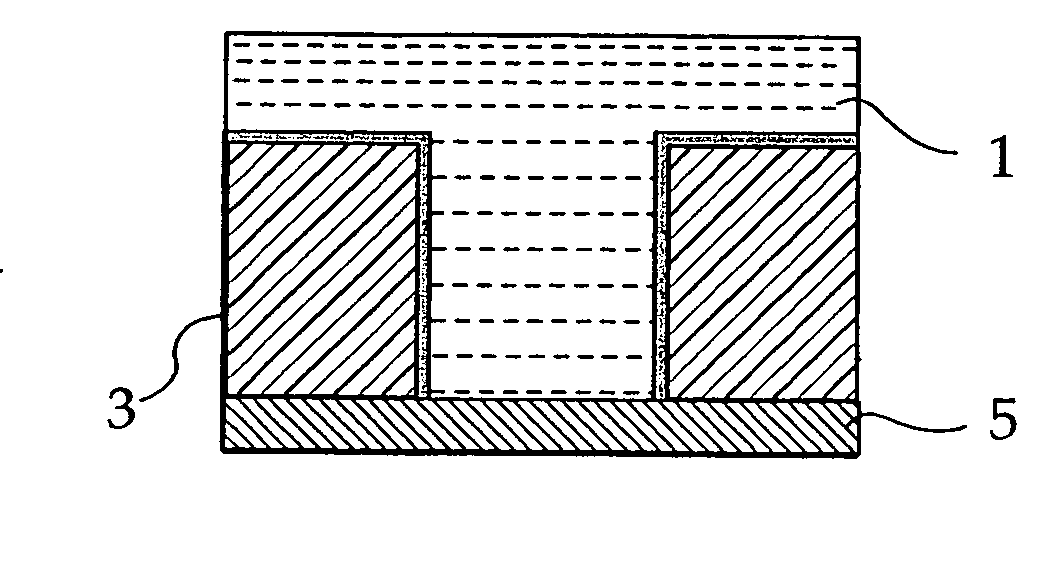
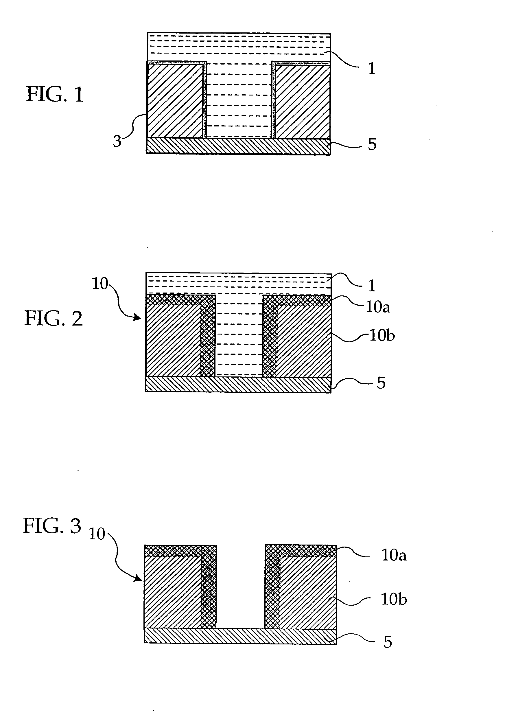
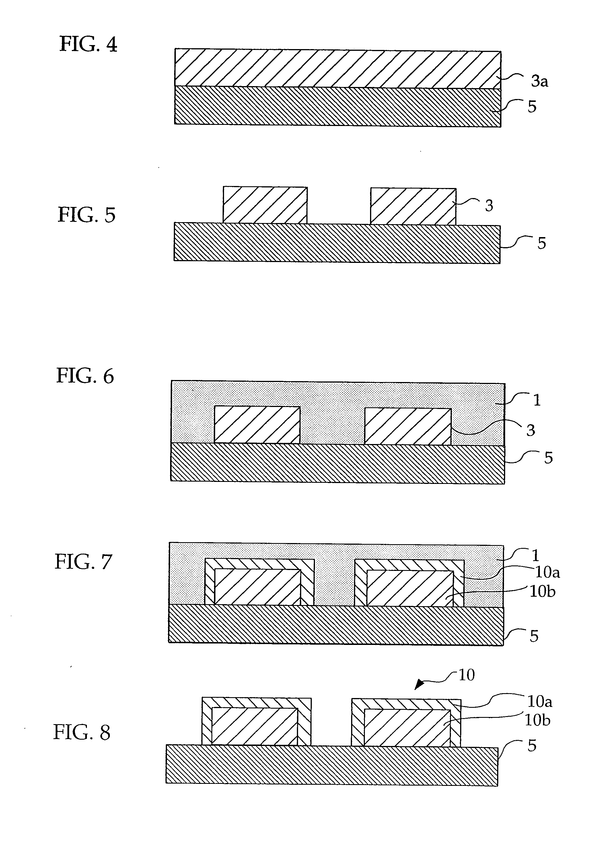
[0018] When the resist pattern thickening material is applied over a resist pattern to be thickened, the portions of the applied resist pattern thickening material in a vicinity of the interface with the resist pattern to be thickened infiltrate into the resist pattern and cause an interaction, i.e., mixing, with the material of the resist pattern to be thickened. Then, because the affinity is high between the resist pattern thickening material and the resist pattern to be thickened, a surface layer or mixing layer, where the resist pattern thickening material and the resist pattern are mixed, is efficiently formed on the surface of the resist pattern as the inner layer. As a result, the resist pattern to be thickened is efficiently thickened by the resist pattern thickening material. The resist pattern thickened in this way (hereinafter sometimes referring to as “thickened resist pattern”) is thickened uniformly by the resist pattern thickening material. Thus, the space pattern of resist formed by the thickened resist pattern a fine space pattern of resist has a fine structure, exceeding exposure limits or resolution limits. The term “space pattern” is hereby defined as a hole, trench, recess, or any other empty space that is formed by developing a resist. Since the resist pattern thickening material of the present invention includes the compound represented by the general formula (1), uniform thickening effect is derived without being affected by the types of resist material or sizes of the resist pattern. Further, since the compound represented by the general formula (1) includes an aromatic ring, the resist pattern thickening material of the present invention has high etch resistance. Thus, the resist pattern thickening material of the present invention can be suitably utilized for forming a resist pattern, such as a lines and spaces pattern, on a wiring layer of LOGIC LSI where various sizes of resist patterns are utilized.
[0019] The process for forming a resist pattern of the present invention includes forming a resist pattern to be thickened, and then coating a resist pattern thickening material of the present invention so as to cover the surface of the resist pattern to be thickened. In the process for forming a resist pattern of the present invention, a resist pattern to be thickened is formed and then, when the resist pattern thickening material is applied over the resist pattern to be thickened, the portions of the applied resist pattern thickening material in a vicinity of the interface with the resist pattern to be thickened infiltrate into the resist pattern and cause an interaction or mixing with the material of the resist pattern. Thus, a surface layer or mixing layer, where the resist pattern thickening material and the resist pattern are mixed, is formed on the surface of the resist pattern as the inner layer. The resulting thickened resist pattern is uniformly thickened by the resist pattern thickening material. Thus, the space pattern of resist formed by the thickened resist pattern a fine space pattern of resist has a fine structure, exceeding exposure limits or resolution limits. Since the resist pattern thickening material includes the compound represented by the general formula (1), uniform thickening effect is derived without...

Problems solved by technology

Specifically, when a resist pattern is swelled using a conventional resist swelling ...

Method used


Image

  • Resist pattern thickening material and process for forming resist pattern, and semiconductor device and process for manufacturing the same
  • Resist pattern thickening material and process for forming resist pattern, and semiconductor device and process for manufacturing the same
  • Resist pattern thickening material and process for forming resist pattern, and semiconductor device and process for manufacturing the same

Examples


example 1

Preparation of Resist Pattern Thickening Material

[0223] Resist pattern thickening materials A through T having the compositions shown in Table 1 were prepared.

[0224] Note that, in Table 1, the “thickening material” means a resist pattern thickening material, and “A” through “T” correspond to the resist pattern thickening materials A through T. Of the resist pattern thickening materials A through T, the resist pattern thickening materials A, B, and P correspond to comparative example and the resist pattern thickening materials C to 0 and Q to T correspond to examples (of the present invention). Note that, in Table 1, the unit of the values in parentheses is parts by mass.

[0225] In the “compound represented by the general formula (1)” column of resist pattern thickening materials C to 0 and Q to T, benzyl alcohol, benzylamine, and a derivative thereof are compounds represented by the following general formula (1).

[0226] In the general formula (1), “X” is a functional group repre...

example 2

[0248] As shown in FIG. 9, an interlayer dielectric film 12 was formed on a silicon substrate 11, and as shown in FIG. 10, a titanium film 13 was formed by a sputtering method on the interlayer dielectric film 12. Next, as shown in FIG. 11, a resist pattern 14 was formed by a known photolithographic technique. By using the resist pattern 14 as a mask, the titanium film 13 was patterned by reactive ion etching to form openings 15a. Reactive ion etching was continuously carried out to remove the resist pattern 14, at the same time, as shown in FIG. 12, openings 15b were formed in the interlayer dielectric film 12 by using the titanium film 13 as a mask.

[0249] Next, the titanium film 13 was removed by wet processing, and as shown in FIG. 13, a TiN film 16 was formed on the interlayer dielectric film 12 by a sputtering method. Subsequently, a Cu film 17 was grown by an electrolytic plating method on the TiN film 16. Next, as shown in FIG. 14, planarizing was carried out by CMP such tha...

example 3

Flash Memory and Manufacture Thereof

[0253] Example 3 illustrates an embodiment of the semiconductor device and the manufacturing process thereof of the present invention using a resist pattern thickening material of the present invention. In Example 3, resist films 26, 27, 29 and 32 are ones thickened by the same method as in Examples 1 and 2 using the resist pattern thickening material of the present invention.

[0254]FIGS. 18 and 19 are top views (plan views) of a FLASH EPROM which is called a FLOTOX type or an ETOX type. FIGS. 20 through 28 are schematic sectional views showing a manufacturing process of the FLASH EPROM. In these figures, the left views are schematic sectional views (sectional views taken along lines A-A) of a memory cell unit (a first element region), in a gate width direction (in the X direction in FIGS. 18 and 19), in a portion where a MOS transistor having a floating gate electrode is to be formed. The central views are schematic sectional views (sectional v...


PUM


Abstract

The present invention provides a resist pattern thickening material, which can utilize ArF excimer laser light; which, when applied over a resist pattern to be thickened e.g., in form of lines and spaces pattern, can thicken the resist pattern to be thickened regardless of the size of the resist pattern to be thickened; and which is suited for forming a fine space pattern or the like, exceeding exposure limits. The present invention also provides a process for forming a resist pattern and a process for manufacturing a semiconductor device, wherein the resist pattern thickening material of the present invention is suitably utilized.

Description

CROSS-REFERENCE TO RELATED APPLICATIONS [0001] This application is based upon and claims the benefits of the priority from the prior Japanese Patent Application No. 2005-042884, filed on Feb. 18, 2005, the entire contents of which are incorporated herein by reference. BACKGROUND OF THE INVENTION [0002] 1. Field of the Invention [0003] The present invention relates to a resist pattern thickening material, which is applied over a resist pattern that is formed in manufacturing a semiconductor device and is capable of thickening the resist pattern, and which may form a fine space pattern that exceeds exposure limits of light sources of available exposure devices. The present invention also relates to a process for forming a resist pattern, a semiconductor device, and a process for manufacturing the semiconductor device that utilize the resist pattern thickening material respectively. [0004] 2. Description of the Related Art [0005] Semiconductor integrated circuits are becoming more high...

Claims


Application Information

Patent Timeline
IPC IPC(8): G03C1/76
CPCG03F7/40
Inventor NOZAKI, KOJINAMIKI, TAKAHISAKOZAWA, MIWA
Owner FUJITSU LTD
Why Eureka
Try Eureka